However, this physical scaling of device sizes raises significant issues, especially in connection with embedded SRAM but also in SRAM realized as “stand-alone” memory
integrated circuit devices.
Several of these issues are due to increased variability in the electrical characteristics of transistors formed at these extremely small feature sizes.
This variability in characteristics has been observed to increase the likelihood of read and write functional failures, on a
cell-by-
cell basis.
The combination of increased device variability with the larger number of memory cells (and thus transistors) within an
integrated circuit renders a
high likelihood that one or more cells cannot be read or written as expected.
These high-k
metal gate n-channel MOS transistors have been observed to be vulnerable to
threshold voltage shifts due to PBTI, even though their conventional
gate dielectric n-channel devices are not.
This
vulnerability is believed due to the affinity of HfO2 films to trap electrons under positive gate bias (relative to the
transistor channel region).
In the context of CMOS SRAMs, BTI degradation affects the ability of memory cells to retain data, and to be written and read.
BTI degradation can cause operational failures in SRAM cells that are already vulnerable due to variability and mismatch of sub-micron minimum feature size transistors, and other factors.
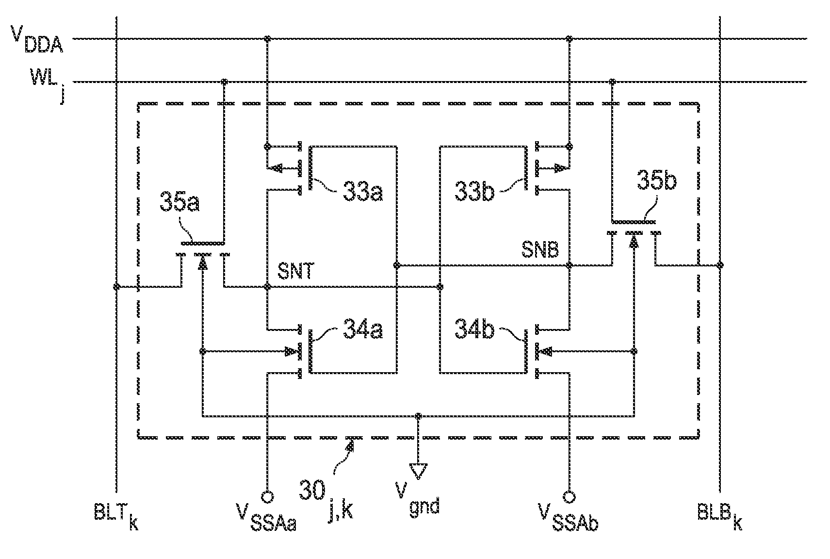
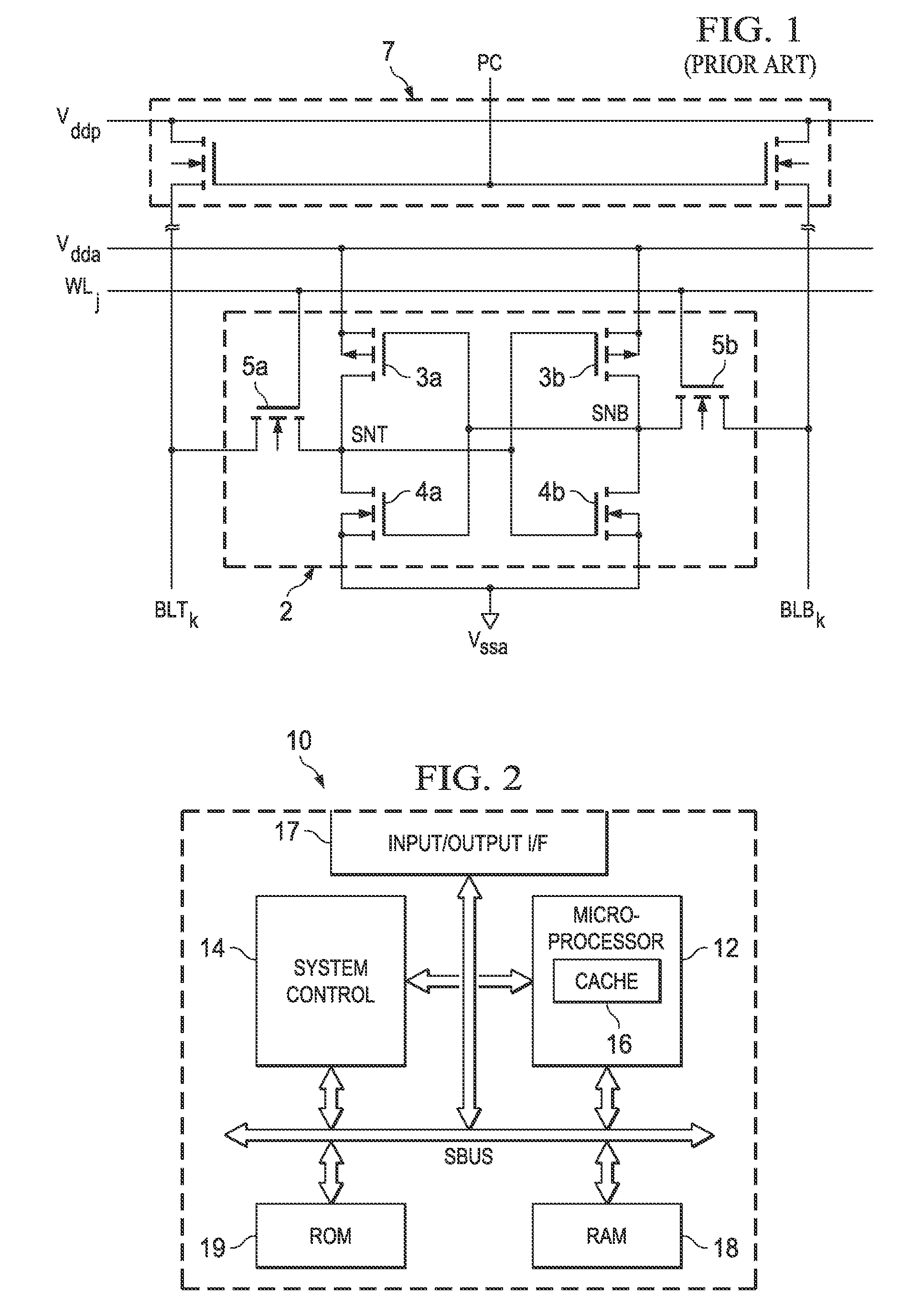
While pass transistors 5a, 5b are also vulnerable to PBTI, the
duty cycle at which these devices are biased on is much lower than for the
inverter transistors.
One type of failure that can be caused by BTI is a read stability failure, also referred to as a “disturb” failure or as insufficient
static noise margin, in which
noise appearing as an elevated
voltage (e.g., 0.2 volts) at the low storage node causes a false change of state of the cell.
If the low side driver transistor is not able to hold a sufficiently
low voltage at the storage node, this
noise can be of sufficient magnitude to trip the inverters of the cell.
Read stability failures can occur in cases in which the drive of the
SRAM cell driver or load transistors is mismatched relative to other transistors in the cell.
Conversely, a long-held “0” data state of cell 2 can cause NBTI degradation at load transistor 3b, increasing its threshold
voltage relative to that of load transistor 3a. The resulting degradation in drive strength of load transistor 3b will reduce its ability to hold storage node SNB to a
high voltage during a
noise event, which also decreases the
static noise margin of cell 2 and increases the likelihood of an undesired change of state.
Sufficiently weak read current will, of course, causes an insufficient differential
signal to be developed across bit lines BLTk, BLBk, leading to a so-called “read failure” (an incorrect data state being read).
SRAM cells that exhibit PBTI and NBTI are vulnerable to a similar
failure mechanism, referred to in the art as a retention stability failure.
This failure is manifest by the cell being unable to retain its stored data state at a reduced
power supply voltage level.
Weakened drive capability due to PBTI in one of the driver transistors, or weakened drive capability due to NBTI on one of the load transistors, contributes to poorer retention capability of an
SRAM cell because of the resulting
weakness with which the levels at the corresponding storage nodes are held by those devices.
Another
failure mechanism that can result from PBTI and NBTI degradation is a write failure, which occurs when an addressed
SRAM cell does not change its stored state in response to a write of the opposite data state from that stored.
Write failures are the converse of read stability failures—while a read stability failure occurs if a cell changes its state too easily, a write failure occurs if a cell is too stubborn in changing its state, specifically by the write circuitry being unable to pull down the storage node that is currently latched to a
high voltage.
As known in the art, it is becoming increasingly difficult to design the appropriate test “vectors” (i.e., combinations of bias and internal circuit voltages, and other test conditions) that identify devices that are vulnerable to failure over time and temperature, without significant yield loss of devices that would not fail over
operating life yet fail the screen at the applied guardbanded test vectors.
To the extent that potential proxies for this effect are available, those proxies necessitate an excessively harsh screen margin (i.e., guardband) to meet modern reliability goals.
The undue yield loss of devices that fail such a screen but would, in fact, not have degraded to failure, can be substantial.

