

Epitaxial substrate and method for manufacturing epitaxial substrate
- Summary
- Abstract
- Description
- Claims
- Application Information
AI Technical Summary
Benefits of technology
Problems solved by technology
Method used
Image

Examples
examples
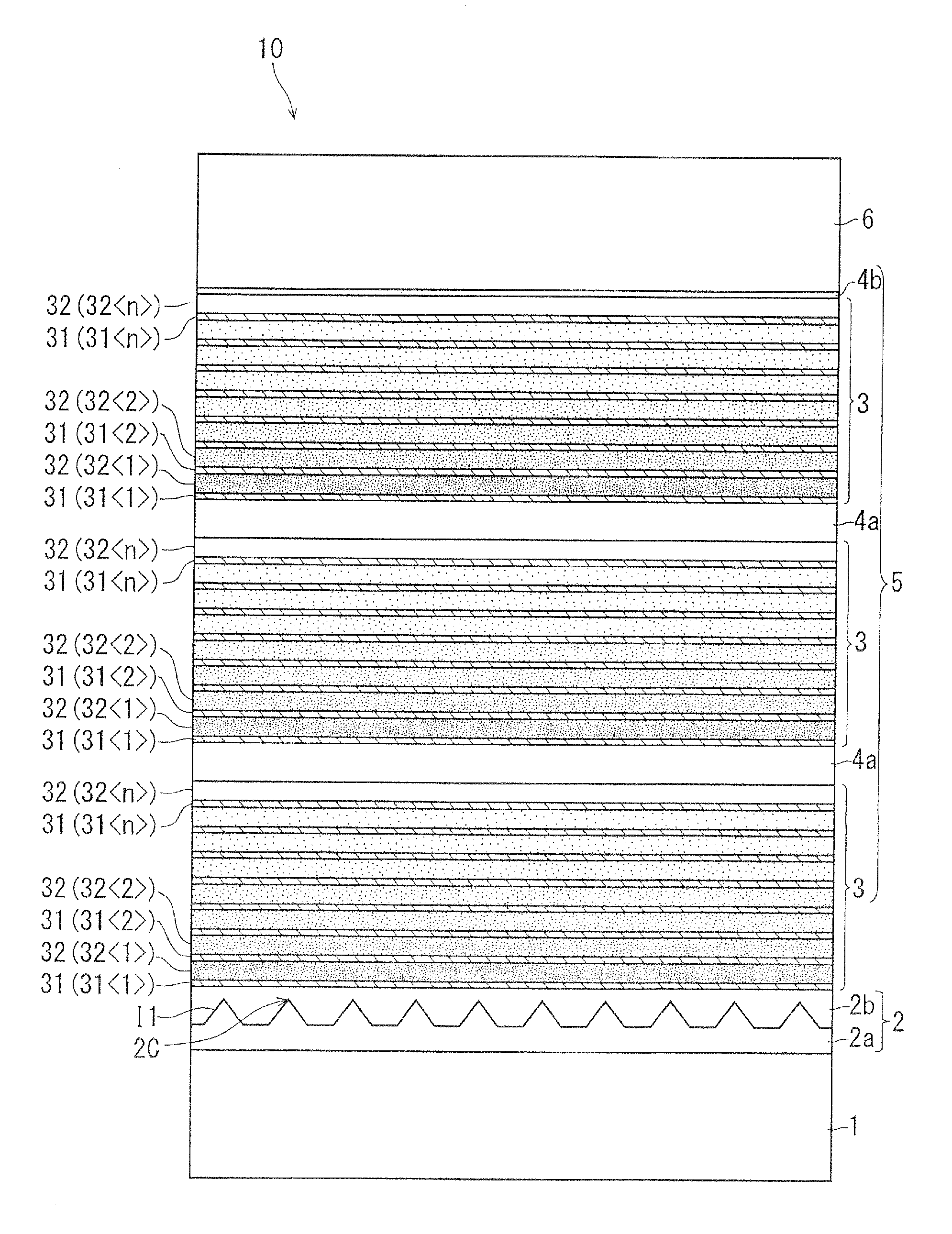
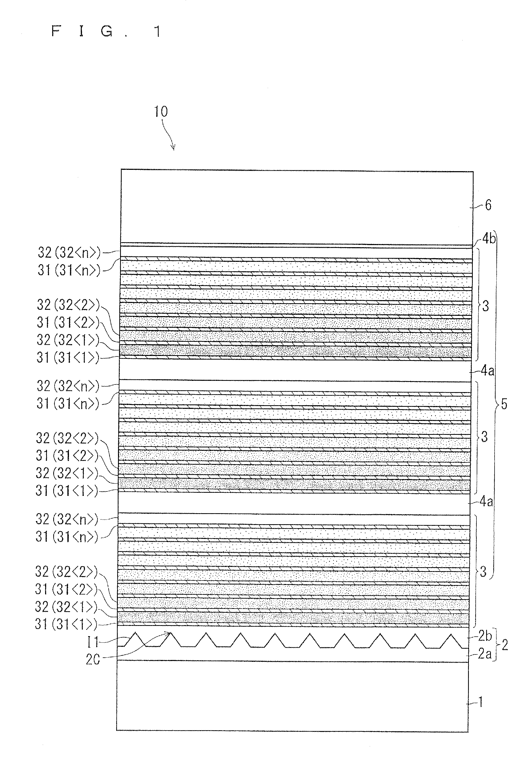
[0107]As an example, a plurality of types of epitaxial substrates 10 were prepared, which were different from one another in terms of the layer configuration of the buffer layer 5. Table 1 shows a basic configuration of the epitaxial substrates 10 according to the example, and more specifically, materials for forming the respective layers and the film thicknesses of the respective layers.
TABLE 1
[0108]As shown in Table 1, in this example, the materials and the film thicknesses of the base substrate 1, the base layer 2 (the first base layer 2a and the second base layer 2b), and the function layer 6 were the same for all the epitaxial substrates 10. The function layer 6 was configured as two layers of the channel layer and the barrier layer.
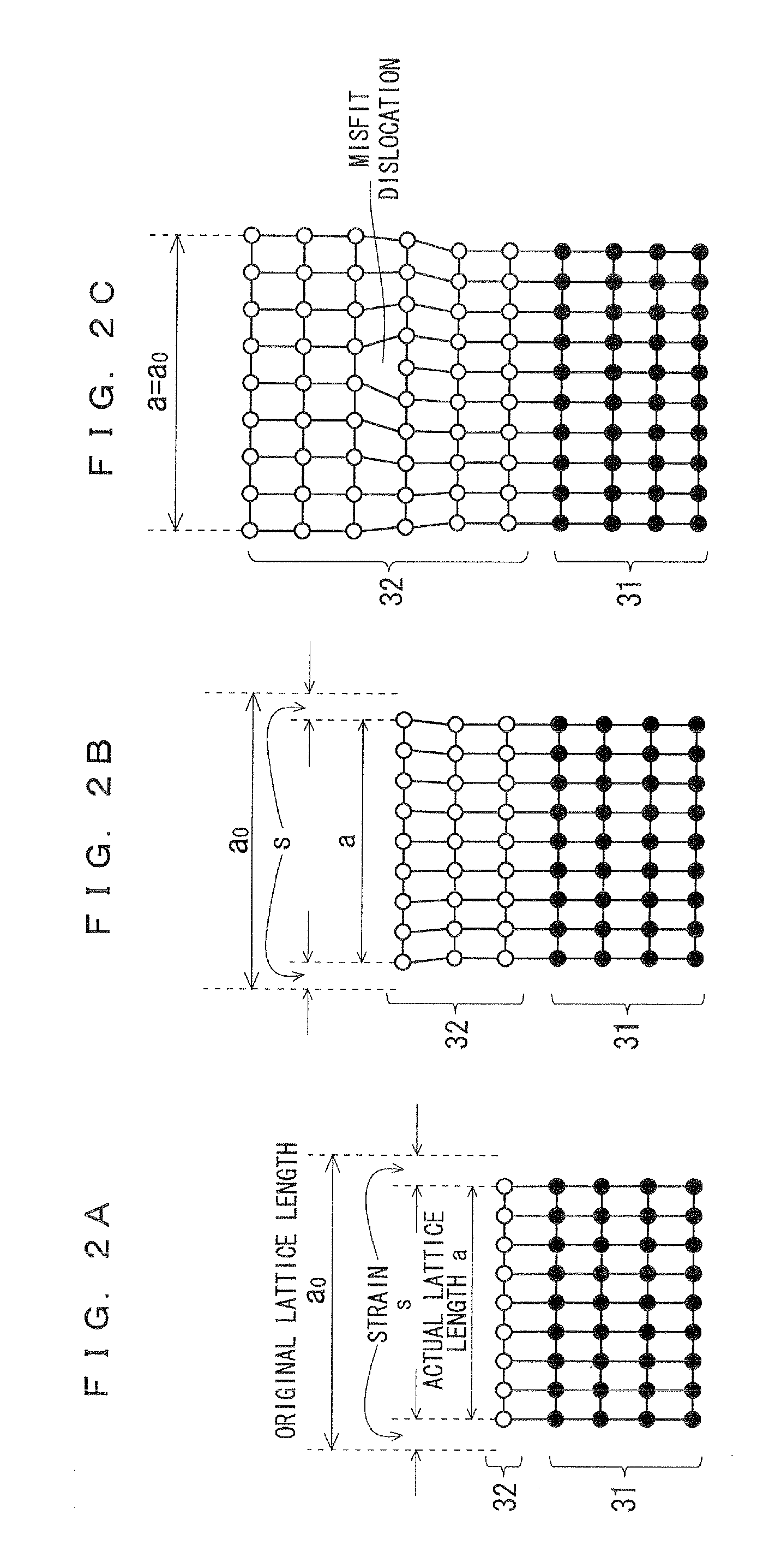
[0109]On the other hand, both the first composition layer 31 and the termination layer 4 were made of AlN, but their film thickness was different among specimens. In Table 1, this is indicated by the variable A (nm). Likewise, the film thickness of ...
PUM
 Abstract
Description
Claims
Application Information