Gate stack structure and fabricating method used for semiconductor flash memory device

a technology of flash memory and gate stack, which is applied in the direction of nanoinformatics, chemical vapor deposition coating, coating, etc., can solve the problems of low programming/erasure speed, high operating voltage, and memory device performance affected, and achieve low operating voltage, fast programming, and high stored-charge density.

Inactive Publication Date: 2013-03-14
FUDAN UNIV
View PDF1 Cites 7 Cited by
  • Summary
  • Abstract
  • Description
  • Claims
  • Application Information

AI Technical Summary

Benefits of technology

[0006]The object of the present invention is to provide a gate stack stricture for use in a semiconductor flash memory device, which has a high stored-charge density, a low operating voltage, fast programming and erasing speeds, as well as good charge retention. The other object of the present invention is to offer a method of fabricating the above-mentioned gate stack structure.

Problems solved by technology

Beyond 65 nm technology node, the conventional poly-silicon floating gate memory device will face many problems, thus the memory device performance will be affected, such as low programming / erasing speed, high operating voltage etc.
However, relatively high operating voltages and slow operating speed are the major drawbacks of the SONOS-type memory.

Method used


Image

  • Gate stack structure and fabricating method used for semiconductor flash memory device
  • Gate stack structure and fabricating method used for semiconductor flash memory device
  • Gate stack structure and fabricating method used for semiconductor flash memory device

Examples


Embodiment Construction

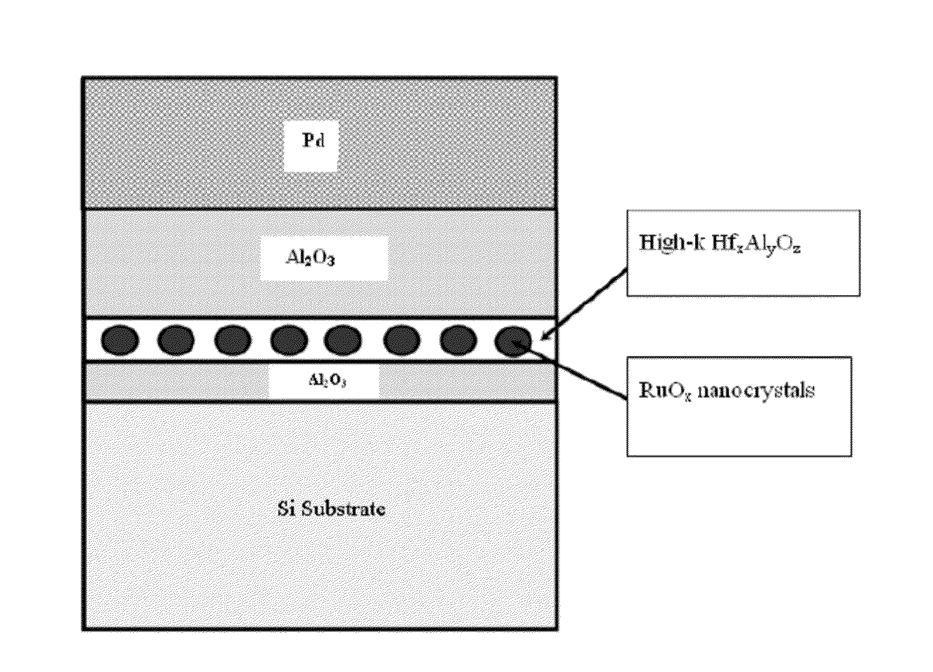
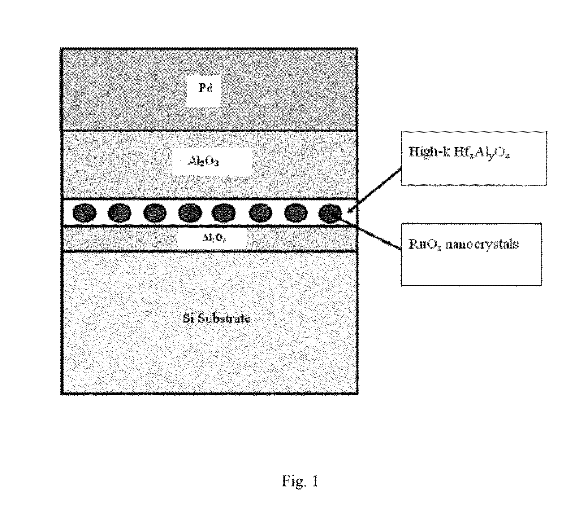
[0043]Referring to FIG. 1, the present invention relates to a gate stack structure for use in a semiconductor flash memory device, in particular, the related gate stack structure contains a heterogeneous charge storage layer consisting of metal nanocrystals and high-k film. Said flash memory capacitor includes the following components in sequence from bottom to top:

[0044](1) A p-type monocrystalline silicon wafer with orientation 100 used as a substrate;

[0045](2) An Al2O3 film with a thickness of 5˜15 nm grown on the silicon substrate by atomic layer deposition, which acts as a tunnel layer;

[0046](3) Said heterogeneous charge storage layer further includes: metal nanocrystals acting as a first charge trapping layer, which is consisting of Ru and Ru oxide (denoted by RuOx nanocyrstals);

[0047]a high-k film with a thickness of 3˜20 nm (preferred thickness is 5˜10 nm) grown by ALD acting as a second charge trapping layer, the dielectric of said high-k is HfxAlyOz, (x>0, z>0 and y=0 or y...


PUM

PropertyMeasurementUnit
thicknessaaaaaaaaaa
thicknessaaaaaaaaaa
thicknessaaaaaaaaaa

Abstract

The invention relates to a gate stack structure suitable for use in a semiconductor flash memory device and its fabricating method. The gate stack structure is fabricated on a p-type 100 silicon substrate, which also includes the following components in sequence from bottom to top: a charge tunnel layer of Al2O3 film, the first charge trapping layer of RuOx nanocrystals; the second charge trapping layer of high-k HxAlyOz film, a charge blocking layer of Al2O3 film, and a top electrode. In this invention, the RuOx nanocrystals have excellent thermal stability, and do not diffuse easily at high temperatures. The high-k HfxAlyOz film has high density charge traps.Pd with a high work function is used as the top electrode. Therefore, the present gate stack structure has vast practical prospects for nanocrystal memory devices.

Description

FIELD OF INVENTION[0001]The present invention relates to the fabrication of semiconductor integrated circuits, and, particularly to an electric capacity structure and a fabricating method of a flash memory capacitor. More specifically, it relates to a gate stack structure and a fabricating method with a novel heterogenous charge storage layer composed of metal nanocrystals and high permittivity (high-k) dielectric.BACKGROUND OF INVENTION[0002]With development of semiconductor process and technology, the integration density of nonvolatile flash memory becomes higher and higher, at the same time, the operating voltage becomes lower and lower. Therefore, these drive a continuous shrinkage of memory device. Beyond 65 nm technology node, the conventional poly-silicon floating gate memory device will face many problems, thus the memory device performance will be affected, such as low programming / erasing speed, high operating voltage etc.[0003]Recently, a new type of nonvolatile memory bas...

Claims


Application Information

Patent Timeline
Patent Type & Authority Applications(United States)
IPC IPC(8): H01L21/28H01L29/792
CPCB82Y10/00H01L21/28079H01L21/28273H01L29/495H01L29/4234C23C16/45525H01L21/28282H01L29/42332C23C16/40H01L29/40114H01L29/40117
Inventor DING, SHIJINGOU, HONGYANZHANG, WEI
Owner FUDAN UNIV
Why Eureka
Try Eureka