High Performance Divider Using Feed Forward, Clock Amplification and Series Peaking Inductors

a technology of high-performance dividers and inductors, applied in differential amplifiers, oscillator generators, pulse automatic control, etc., can solve the problems of cmos divide by 2 suffering from rc delay, difficult design of high-performance systems in low-power supply integrated circuits, etc., to increase the dynamic range of applied signals, increase the headroom of differential amplifiers, and reduce the voltage headroom of analog integrated circuits

Active Publication Date: 2013-03-28
TENSORCOM
View PDF2 Cites 7 Cited by
  • Summary
  • Abstract
  • Description
  • Claims
  • Application Information

AI Technical Summary

Benefits of technology

[0007]As the power supply voltage reduces in the scaling of integrated circuits, the voltage headroom for analog integrated circuits decreases correspondingly. This makes the design of high performance systems in a low power supply integrated circuit much more difficult and challenging. The CMOS VCO (Voltage Controlled Oscillator) in the PLL can generate a clock signal operating in the 60 GHz range of frequencies at reduced supply voltages. This clock signal needs to be divided down to a more manageable frequency before the remainder of the circuits on the chip can use this divided down clock signal. A divide by 2 is one of the first circuits to reduce the frequency of the clock signal to a more manageable frequency. The divide by 2 divides the high frequency clock signal (f) in half to generate a clock signal operating at half of the high frequency signal (f / 2). Note that the divide by 2 must be clocked at the high frequency rate (f). The period of a 60 GHz clock is about 16.6 ps while the delay through a device or transistor is slightly more than this. Thus, if conventional CMOS circuit techniques are applied to the divide by 2 clocked at 60 GHz, conventional CMOS circuit techniques would prevent the operation of the divide by 2 since the delay through one CMOS device is larger than the clock period. This explains why designers are steered to the injection locked divider technique. Our technique offers a robust divide by 2 without resorting to the injection locked divider technique.
[0008]One of the embodiments of the disclosure removes the series bias transistor thereby increasing the headroom of differential amplifier. The increased headroom increases the dynamic range of applied signals. This feature allows faster performing circuits.
[0009]The conventional CMOS divide by 2 suffers from an RC delay caused by the capacitive load across the resistive load. A series peaking inductor is incorporated into each leg of the amplifier to tune out the output capacitance load that is coupled to the output of the differential amplifier. This effectively eliminates the RC delay thereby improving the performance of the circuit.
[0010]Another embodiment use vector summation of two orthogonal clocks to create a composite clock signal that has an amplitude that is 41% larger. This clock signal is used to enable / disable (switch) the differential amplifier and differential memory of a flip flop. The increased amplitude of the composite clock signal increases the gate to source voltage applied to the switched transistor causing the composite clock signal to improve the performance of the circuit.
[0011]An embodiment uses feed forward to a clocked differential amplifier. However, the feed forward path is not clocked. Instead, a current source regulates the current flow through the feed forward circuit. A current mirror can vary the current through the feed forward circuit. This current can be reduced to 0 or varied to shift the resonant behavior of the RLC load. The first case removes the feed forward circuit's behavior by tri-stating the feed forward circuit while the second case can be used to improve performance of the divide by 2 or adjust the resonant circuit characteristics of the RLC circuit.

Problems solved by technology

This makes the design of high performance systems in a low power supply integrated circuit much more difficult and challenging.
The conventional CMOS divide by 2 suffers from an RC delay caused by the capacitive load across the resistive load.

Method used


Image

  • High Performance Divider Using Feed Forward, Clock Amplification and Series Peaking Inductors
  • High Performance Divider Using Feed Forward, Clock Amplification and Series Peaking Inductors
  • High Performance Divider Using Feed Forward, Clock Amplification and Series Peaking Inductors

Examples


Embodiment Construction

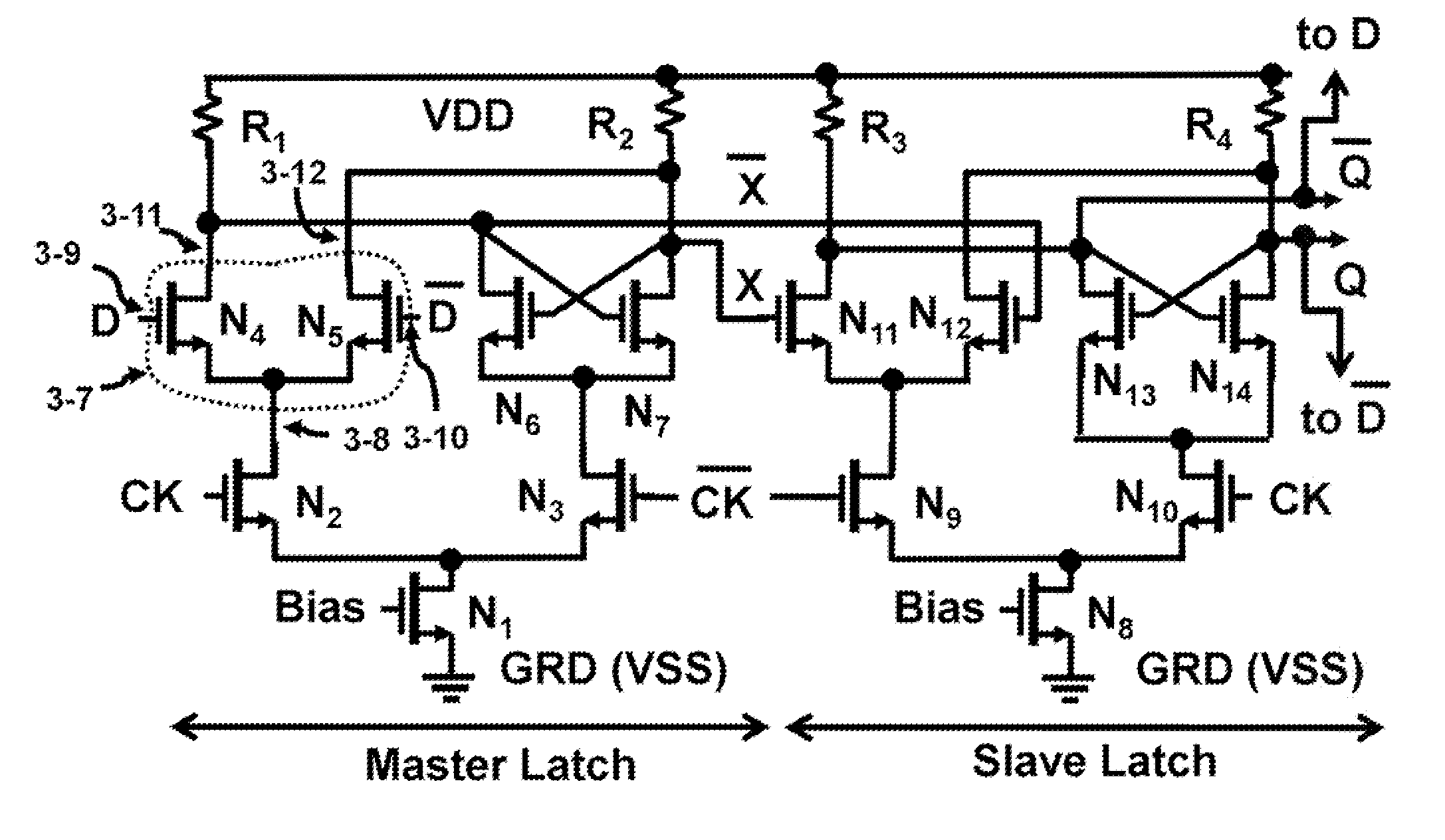
[0034]The inventions presented in this specification can be used in high frequency system designs. Several embodiments are presented where any combination of these embodiments can be included into the circuit design. Although a divide by 2 is illustrated as benefiting from these techniques, these techniques can also be applied to other high speed circuits.

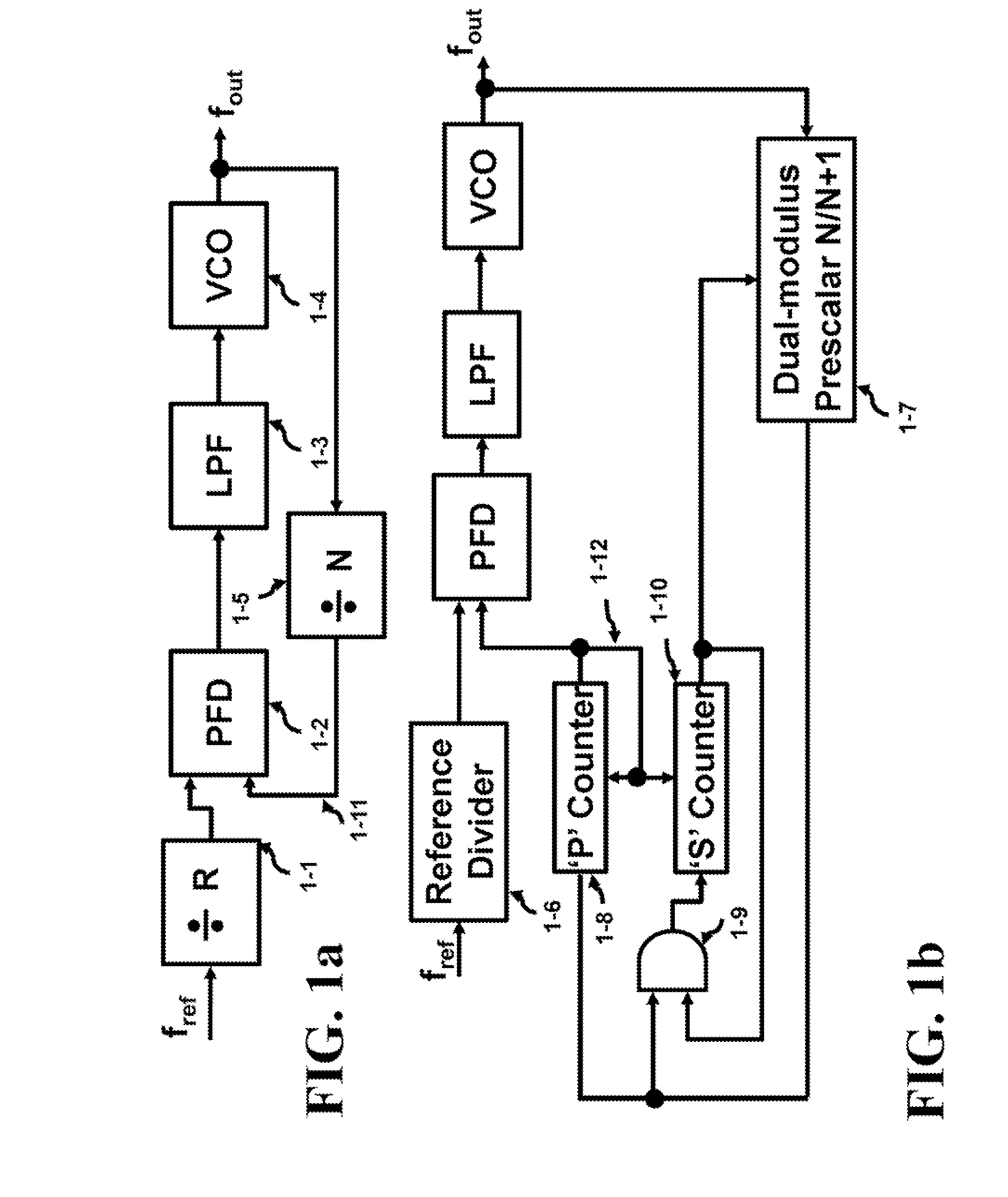
[0035]FIG. 1a illustrates a conventional PLL. The reference frequency from a crystal of fref is divided down by the divide by R block 1-1. The low frequency signal is compared in the PDF (Phase and Frequency Detector) against the variable clock signal 1-11. The VCO 1-4 generates the high frequency signal fout. This signal is presented to the prescalar 1-5 and is divided by N and compared against a reference signal in the PFD block 1-2. The output of the PFD is low pass filtered (LPF 1-3) to generate a DC voltage that is applied to the VCO to adjust the high frequency signal fout.

[0036]In FIG. 1b, a dual modulus prescalar is present...


PUM


Abstract

A phase lock loop (PLL) is an important component in wireless systems. CMOS technology offers voltage controlled oscillator designs operating at 60 GHz. One of the difficulties is dividing the high frequency clock down to a manageable clock frequency using conventional CMOS. Although injection locked dividers can divide down this clock frequency, these dividers have limitations. A divide by 2 is presented that uses several techniques; feed forward, clock amplification and series peaked inductors to overcome these limitations.

Description

CROSS REFERENCE TO RELATED APPLICATIONS[0001]The present application is related to the co-filed U.S. application entitled “A Differential Source Follower having 6dB Gain with Applications to WiGig Base hand Fillers”, and the co-filed U.S. application entitled “Method and Apparatus of Minimizing Extrinsic Parasitic Resistance in 60 GHz Power Amplifier Circuits” both filed on Sep. 23, 2011, which are invented by the same inventor as the present application and incorporated herein by reference in their entireties.BACKGROUND OF THE INVENTION[0002]The Federal Communications Commission (FCC) has allotted a spectrum of bandwidth in the 60 GHz frequency range (57 to 64 GHz). The Wireless Gigabit Alliance (WiGig) is targeting the standardization of this frequency band that will support data transmission rates up to 7 Gbps. Integrated circuits, formed in semiconductor die, offer high frequency operation in this millimeter wavelength range of frequencies. Some of these integrated circuits util...

Claims


Application Information

Patent Timeline
Patent Type & Authority Applications(United States)
IPC IPC(8): H03B19/00H03F3/45
CPCH03L7/193H03K21/023
Inventor SOE, ZAW
Owner TENSORCOM
Why Eureka
Try Eureka