Method for fabrication of crack-free ceramic dielectric films

Active Publication Date: 2013-04-04
UCHICAGO ARGONNE LLC
View PDF2 Cites 2 Cited by
  • Summary
  • Abstract
  • Description
  • Claims
  • Application Information

AI Technical Summary

Benefits of technology

The present invention provides a process for making a crack-free ceramic film with a specific thickness range and a higher dielectric constant compared to typical processes. The process involves applying layers of a precursor to a substrate, heat treating them to reduce thermal stresses, coalescing the layers to form a continuous dense material, and forming a pyrolysis and crystallization step for each layer until the film reaches the desired thickness. The process can be used with different dielectric film forming materials and substrates. The resulting crack-free film has a lower dielectric constant compared to films made by typical processes.

Problems solved by technology

The utilization of ferroelectric thin films for electronic and optical applications has been hindered by the lack of production processes to form deposits of sufficient thickness.
In power electronics, capacitors with high capacitance are required to work at high voltages, typically in the range of 450 to 600 V. This requirement imposes an additional challenge to fabricate thicker films (>1 μm) that can withstand high voltage.
However, in the fabrication process, the deposited films crack easily during heat treatment, due to the well-known critical thickness effect.
Due to this effect per-layer thickness that can be achieved by conventional sol-gel methods is generally limited to about 0.2 μm, thus making these methods unattractive to industry if thicker films are needed.
The efficient removal of decomposition byproducts produced by processing aids during dielectric fabrication and the consolidation of the film raises significant processing issues.

Method used


Image

  • Method for fabrication of crack-free ceramic dielectric films
  • Method for fabrication of crack-free ceramic dielectric films
  • Method for fabrication of crack-free ceramic dielectric films

Examples


Embodiment Construction

[0022]The foregoing summary, as well as the following detailed description of certain embodiments of the present invention, will be better understood when read in conjunction with the appended drawings.

[0023]As used herein, an element or step recited in the singular and preceded with the word “a” or “an” should be understood as not excluding plural said elements or steps, unless such exclusion is explicitly stated. Furthermore, references to “one embodiment” of the present invention are not intended to be interpreted as excluding the existence of additional embodiments that also incorporate the recited features. Moreover, unless explicitly stated to the contrary, embodiments “comprising” or “having” an element or a plurality of elements having a particular property may include additional such elements not having that property.

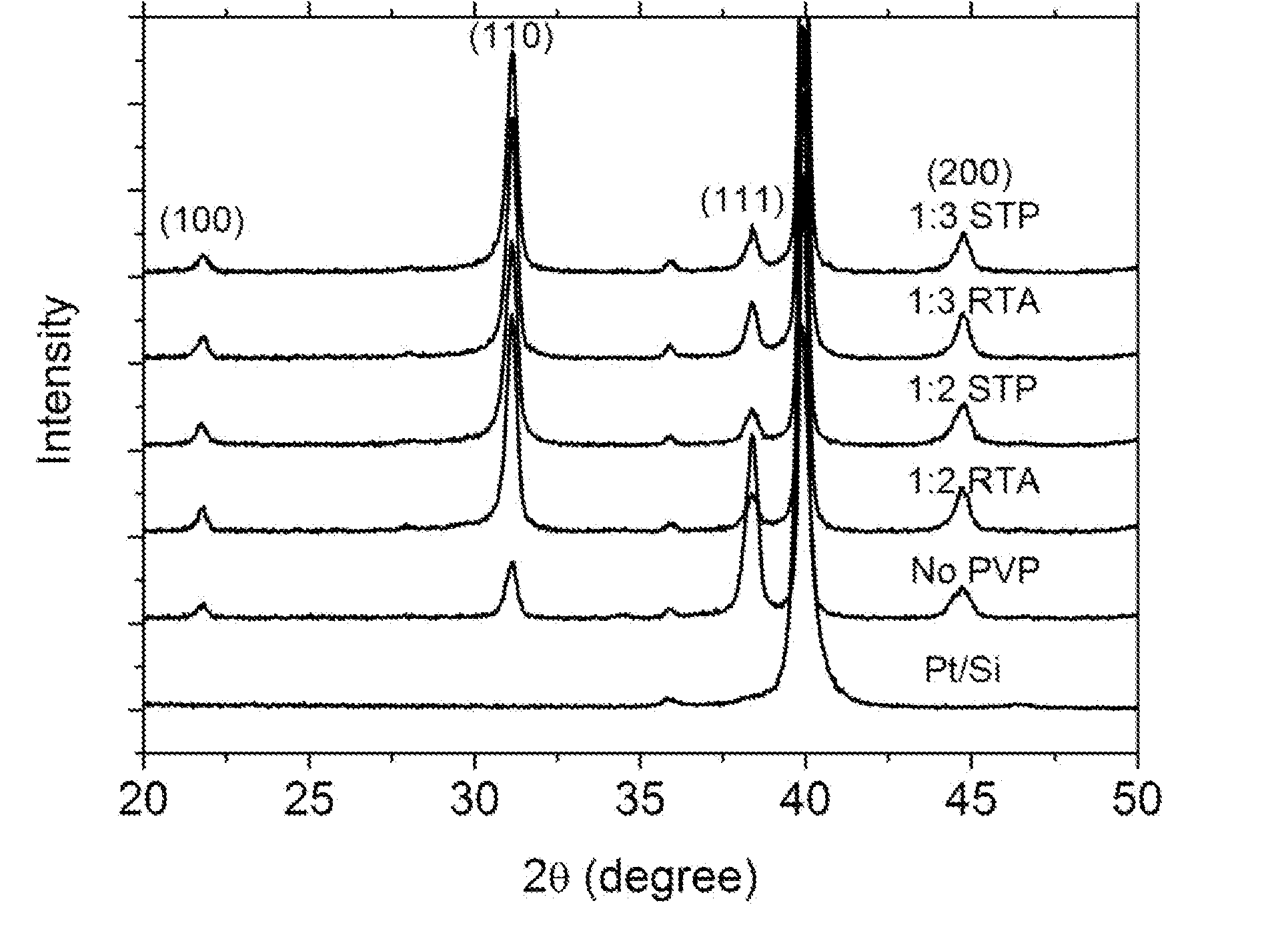
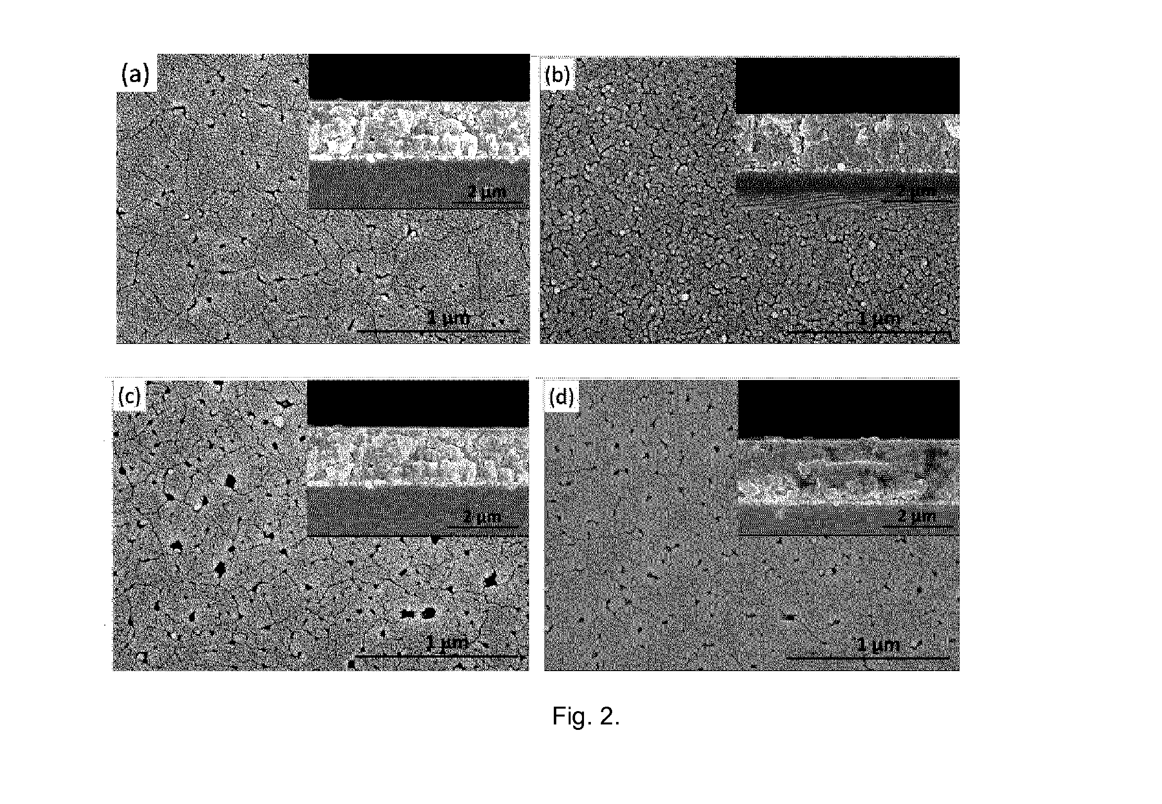
[0024]Dielectric films are used in electrical components, particularly capacitors, to inhibit / control the flow of electricity for power management applications...


PUM

PropertyMeasurementUnit
Temperatureaaaaaaaaaa

Abstract

The invention provides a process for forming crack-free dielectric films on a substrate. The process comprise the application of a dielectric precursor layer of a thickness from about 0.3 μm to about 1.0 μm to a substrate. The deposition is followed by low temperature heat pretreatment, prepyrolysis, pyrolysis and crystallization step for each layer. The deposition, heat pretreatment, prepyrolysis, pyrolysis and crystallization are repeated until the dielectric film forms an overall thickness of from about 1.5 μm to about 20.0 μm and providing a final crystallization treatment to form a thick dielectric film. Also provided was a thick crack-free dielectric film on a substrate, the dielectric forming a dense thick crack-free dielectric having an overall dielectric thickness of from about 1.5 μm to about 20.0 μm.

Description

CONTRACTUAL ORIGIN OF THE INVENTION[0001]The U.S. Government has rights in this invention pursuant to Contract No. DE-AC02-06CH11357 between the U.S. Department of Energy and the University of Chicago representing Argonne National Laboratory.FIELD OF THE INVENTION[0002]The present invention relates to formation of thick ceramic dielectric films. More specifically this invention relates to the formation of thick crack-free ceramic dielectric films, such as lanthanum doped lead zirconate titanate (PLZT) or barium strontium titanate (BST), having an overall thickness of from 1.5 to about 20 μm.BACKGROUND OF THE INVENTION[0003]The recent need for passive power electronics with improved performance, high reliability, and reduced size and weight, has driven interest in ceramic film on metallic substrates in these applications. The ceramic films on metal foils, known as “film-on-foil” technology, in which ceramic films were deposited on base metal foils for embedding into a printed circuit...

Claims


Application Information

Patent Timeline
IPC IPC(8): B05D5/12B32B7/02
CPCB32B7/02Y10T428/24975H01L21/02118H01L21/02186H01L21/02189H01L21/02192H01L21/02194H01L21/02282H01B3/00C04B35/4682C04B35/493C04B35/624C04B35/634C04B2235/3213C04B2235/3227C04B2235/6562C23C18/1225C23C18/1254C23C18/1283C23C18/208H01L21/02197H01B19/04C23C18/1216C23C18/1241C23C18/1295H01L21/02356H01L21/3105H01L28/55
Inventor MA, BEIHAIBALACHANDRAN, UTHAMALINGAMCHAO, SHENGLIU, SHANSHANNARAYANAN, MANOJ
Owner UCHICAGO ARGONNE LLC
Why Eureka
Try Eureka