Reconfigurable high speed memory chip module and electronics system device

a memory chip module and high-speed technology, applied in the direction of solid-state devices, instruments, basic electric elements, etc., can solve the problems of poor heat dissipation, less flexibility, and higher system migration costs among different process technology generations and different applications, so as to improve heat dissipation, improve external noise isolation function, and improve heat dissipation effect

Active Publication Date: 2013-04-11
ETRON TECH INC
View PDF13 Cites 39 Cited by
  • Summary
  • Abstract
  • Description
  • Claims
  • Application Information

AI Technical Summary

Benefits of technology

[0009]The present invention provides a high speed memory chip module and an electronics system device with a high speed memory chip module. The high speed memory chip module and the electronics system device have advantages at least as follows: firstly, because this invention comprises a first transmission bus has a first programmable transmitting or receiving data rate, a first programmable transmitting or receiving signal swing, a first programmable bus width including a first programmable data width, a first programmable address width, and a combination thereof, and a second transmission bus has a second programmable transmitting or receiving data rate, a second programmable transmitting or receiving signal swing, a second programmable bus width including a second programmable data width, a second programmable address width, and a combination thereof, as a result, the present invention has lower power consumption given the performance requirements, higher transmission efficiency given the power limitations, lower cost, higher manufacturability, less technology migration effort, wider application ranges and higher overall performance while operating. Those embodiments can be applied to various ASIC processors (or various SOC processors); and secondly, because the present invention can utilize a plurality of TSVs exist within a non-active circuit region of each memory cell array IC or a plurality of TSVs exist within a non-active circuit region of a logic unit to form a metal fence, comparing to the prior art, the present invention has better EMI shielding effect, better heat dissipation capability, and an better external noise isolation function based on the magnetic-electronic theory available today.

Problems solved by technology

Those common standards, including its well known function or definition about the bus width, signal levels and operating frequency limitations, dictated the memory bus width, the given signal swing and transmission data rate which resulted in lower manufacturability, less flexibility and higher system migration cost among different process technology generations and different applications.
That is to say, a chip or module memory system, integrating discrete memories with the advanced semiconductor process generations, may face poorer heat dissipation, higher power consumption and bad noise interference, so the chip or module memory system with integrating memories and logic units still suffers from much manufacturing difficulty.

Method used


Image

  • Reconfigurable high speed memory chip module and electronics system device
  • Reconfigurable high speed memory chip module and electronics system device
  • Reconfigurable high speed memory chip module and electronics system device

Examples


Embodiment Construction

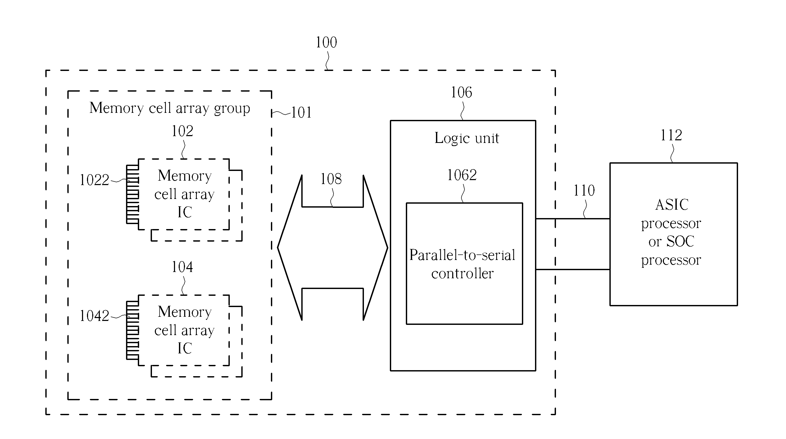
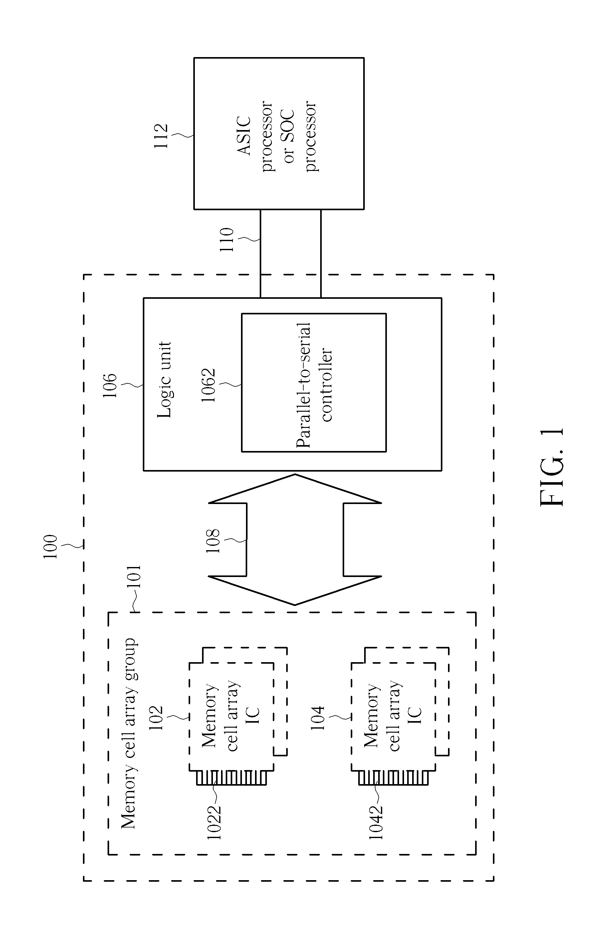
[0026]Please refer to FIG. 1. FIG. 1 is a diagram illustrating a high speed memory chip module 100 according to an embodiment. The high speed memory chip module 100 includes a type of memory cell array group 101, a first transmission bus 108, and a logic unit 106, where the type of memory cell array group 101 includes a memory cell array integrated circuit (IC) 102 which is a Dynamic Random Access Memory (DRAM) IC and a memory cell array IC 104 which is a flash or non-volatile memory (NVM) IC (e.g. a phase-change random access memory (PCRAM), a resistive random access memory (RRAM), an electrically-erasable programmable read-only memory (EEPROM), an erasable programmable read-only memory (EPROM), a magnetoresistive random access memory (MRAM), and so on). But, the present invention is not limited to the high speed memory chip module 100 including the type memory cell array group 101 which includes the memory cell array IC 102 and the memory cell array IC 104, and also not limited to...


PUM


Abstract

A reconfigurable high speed memory chip module includes a type of memory cell array group, a first transmission bus, and a logic unit. The type memory cell array group includes multiple memory cell array integrated circuits (ICs). The first transmission bus coupled to the type memory cell array group has a first programmable transmitting or receiving data rate, a first programmable transmitting or receiving signal swing, a first programmable bus width, and a combination thereof. The logic unit is coupled to the first transmission bus for accessing the type memory cell array group through the first transmission bus.

Description

CROSS REFERENCE TO RELATED APPLICATIONS[0001]This application claims the benefit of U.S. Provisional Application No. 61 / 555,468, filed on Nov. 3, 2011 and entitled “Reconfigurable system-in-package memory platform,” and is a continuation-in-part application of U.S. application Ser. No. 13 / 649,131, filed on Oct. 11, 2012 and entitled “HIGH SPEED MEMORY CHIP MODULE AND ELECTRONICS SYSTEM DEVICE WITH A HIGH SPEED MEMORY CHIP MODULE, ” which claims the benefit of U.S. Provisional Application No. 61 / 546,039, filed on Oct. 11, 2011 and entitled “High Speed Memory Platform.” The disclosures of the prior applications are incorporated herein by reference herein in their entirety.BACKGROUND OF THE INVENTION[0002]1. Field of the Invention[0003]The present invention relates to a high speed memory chip module and a electronics system device with a high speed memory chip module, and particularly to a high speed memory chip module and an electronics system device with a high speed memory chip modu...

Claims


Application Information

Patent Timeline
Patent Type & Authority Applications(United States)
IPC IPC(8): G06F13/42
CPCG06F13/42H01L2924/3025H01L2924/00H01L23/544H01L23/585H01L25/0652H01L25/0657H01L25/18H01L2224/16146H01L2224/16227H01L2224/17181H01L2224/48227H01L2225/0651H01L2225/06517H01L2924/15311H01L2225/06513H01L2225/06541H01L2223/5442H01L2223/54426H01L2223/54473G06F13/4234G06F13/4018Y02D10/00G11C5/06G11C8/18
Inventor KEN, WENG-DAHLU, NICKYSUNG, JAN-MYE
Owner ETRON TECH INC
Why Eureka
Try Eureka