Low energy etch process for nitrogen-containing dielectric layer

Inactive Publication Date: 2013-05-02
ZEON CORP +1
View PDF16 Cites 39 Cited by
  • Summary
  • Abstract
  • Description
  • Claims
  • Application Information

AI Technical Summary

Benefits of technology

[0006]A stack that includes, from bottom to top, a nitrogen-containing dielectric layer, an interconnect level dielectric material layer, and a hard mask layer is formed on a substrate. The hard mask layer and the interconnect level dielectric material layer are patterned by an etch. Employing the patterned hard mask layer as an etch mask, the nitrogen-containing dielectric layer is patterned by a break-through anisotropic etch, which employs a

Problems solved by technology

“Trench-first” BEOL applications suffer issues due to residue formation with exposed metal surfaces, metallic hard-mask retention, and damage to low-k m

Method used


Image

  • Low energy etch process for nitrogen-containing dielectric layer
  • Low energy etch process for nitrogen-containing dielectric layer
  • Low energy etch process for nitrogen-containing dielectric layer

Examples


first embodiment

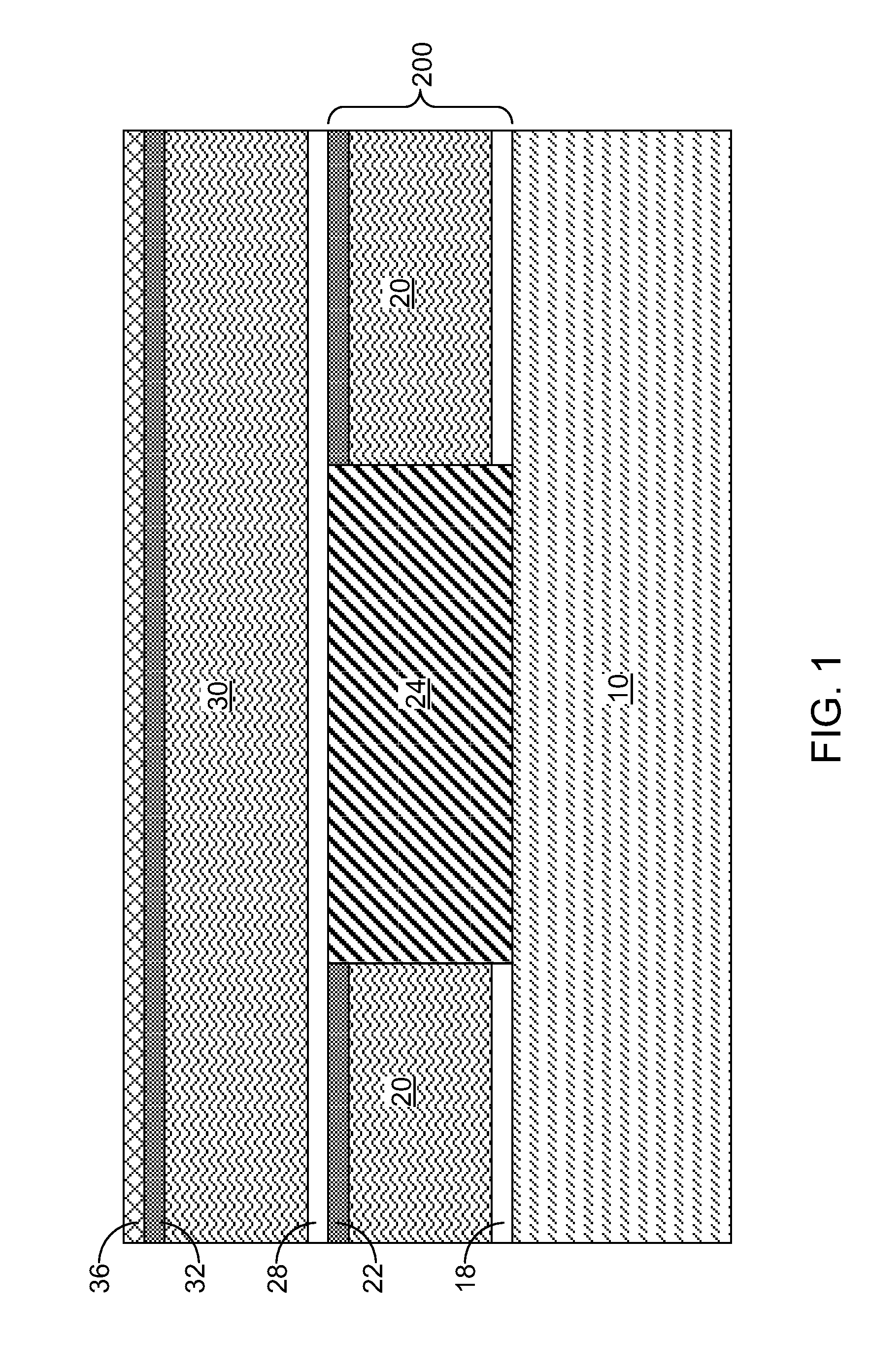
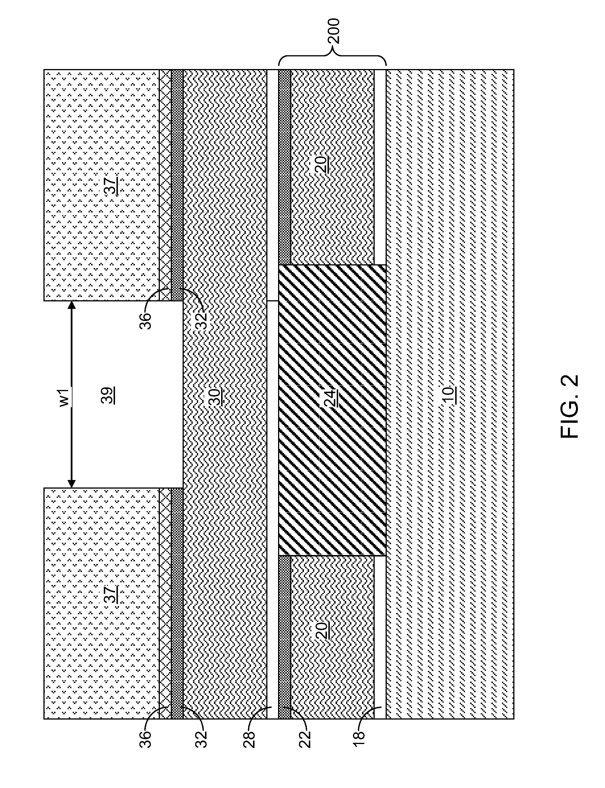
[0025]Referring to FIG. 1, a first exemplary structure according to the present disclosure includes a vertical material stack. The vertical material stack includes a substrate 10, an optional underling metal interconnect level structure 200, a nitrogen-containing dielectric layer 28, an interconnect level dielectric layer 30, a dielectric cap layer 32, and a metallic hard mask layer 36.

[0026]The substrate 10 can include a semiconductor material, an insulator material, a conductive material, or a combination thereof. The semiconductor material can be an elemental semiconductor material such as silicon, germanium, carbon, or an alloy thereof, a III-V compound semiconductor material, a II-VI compound semiconductor material, or any combination or stack thereof. The semiconductor material can be doped with electrical dopants such as B, Ga, In, P, As, and Sb. Multiple semiconductor materials can be present in the substrate. The insulator material can be doped or undoped silicon oxide, dop...

second embodiment

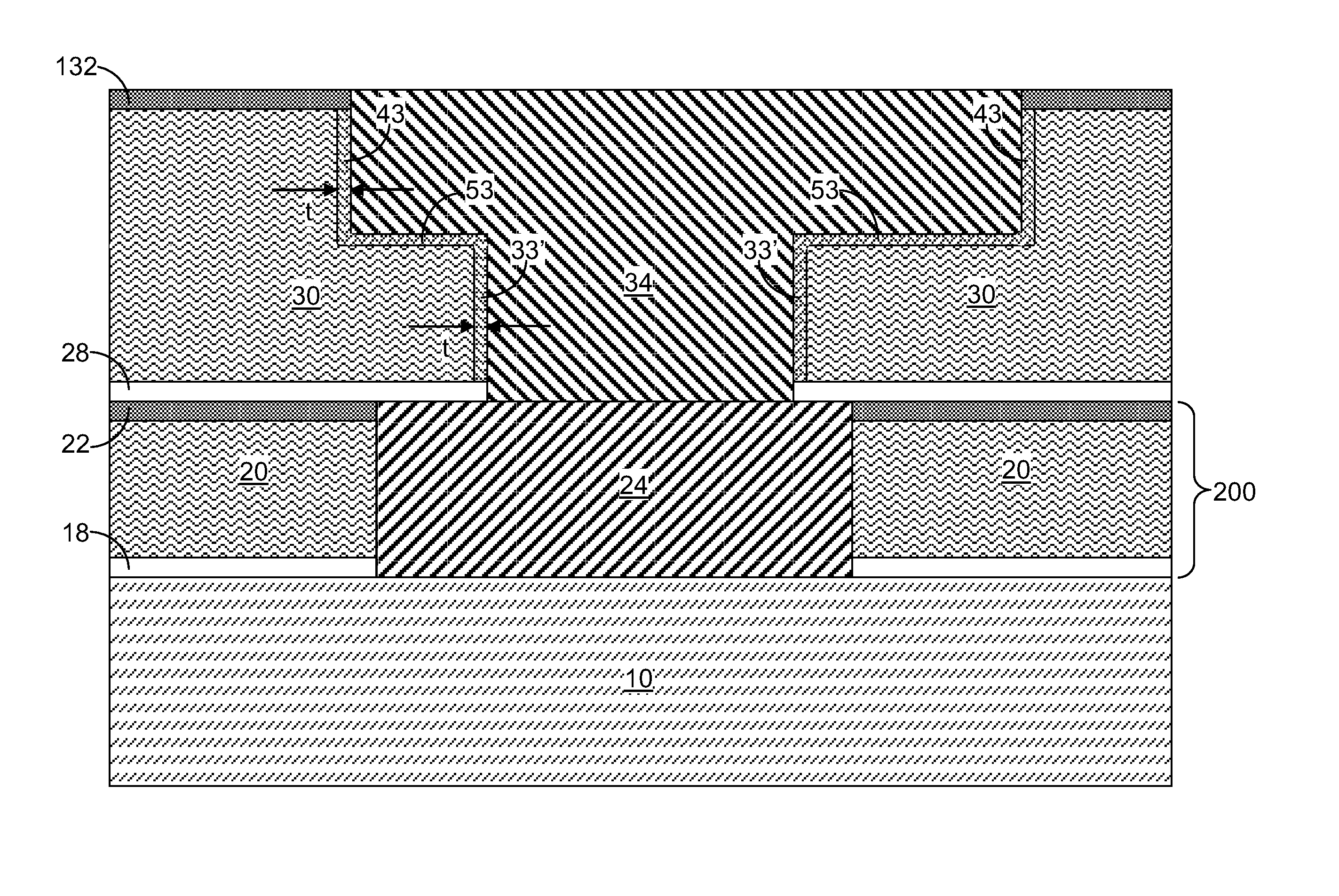
[0067]Referring to FIG. 9, a second exemplary structure according to the present disclosure can be derived from the first exemplary structure of FIG. 1, and by modifying the processing steps of FIG. 2 such that the cavity 31 does not extend to the top surface of the nitrogen-including dielectric layer 28 at the end of the pattern transfer from the photoresist 37 to the upper portion of the interconnect level dielectric layer 30. The cavity 31 as formed within the second exemplary structure is herein referred to as a via cavity 31′. Thus, there is a finite distance between the bottom surface of the via cavity 31′ and the top surface of the nitrogen-containing dielectric layer 28 after removal of the photoresist 37 at the processing step corresponding to the processing step of FIG. 3. The vertical distance between the topmost surface of the interconnect level dielectric layer 30 and the bottom surface of the via cavity 31′ can be from 15% to 85% of the vertical distance between the to...


PUM


Abstract

A stack that includes, from bottom to top, a nitrogen-containing dielectric layer, an interconnect level dielectric material layer, and a hard mask layer is formed on a substrate. The hard mask layer and the interconnect level dielectric material layer are patterned by an etch. Employing the patterned hard mask layer as an etch mask, the nitrogen-containing dielectric layer is patterned by a break-through anisotropic etch, which employs a fluorohydrocarbon-containing plasma to break through the nitrogen-containing dielectric layer. Fluorohydrocarbon gases used to generate the fluorohydrocarbon-containing plasma generate a carbon-rich polymer residue, which interact with the nitrogen-containing dielectric layer to form volatile compounds. Plasma energy can be decreased below 100 eV to reduce damage to physically exposed surfaces of the interconnect level dielectric material layer.

Description

BACKGROUND[0001]The present disclosure relates to semiconductor processing methods, and particularly to methods for anisotropically etching a nitrogen-containing dielectric layer at low energy, and structures for effecting the same.[0002]“Trench-first” BEOL applications suffer issues due to residue formation with exposed metal surfaces, metallic hard-mask retention, and damage to low-k materials such as organosilicate glass throughout the pattern transfer process. Residual fluorine is usually linked to residue formation as well as low-k damage. However, residual fluorine is needed to provide sufficient etch rate for the material of a cap layer during the final stage of the pattern transfer process.[0003]Increasing hard mask retention through process optimization is challenging. Thus, there is a lower limit on the initial thickness of the hard mask that can be employed for adequate lithography process window.[0004]Deposition of removable sidewall polymer deposition to impede damage t...

Claims


Application Information

Patent Timeline
IPC IPC(8): H01L23/48H01L21/768
CPCH01L21/76802H01L21/76813H01L21/76831H01L21/3212H01L21/76835H01L21/31116H01L21/31144H01L21/76834H01L2924/0002H01L2924/00H01L23/5226H01L23/528H01L23/53295
Inventor BRINK, MARKUSBRUCE, ROBERT L.ENGELMANN, SEBASTIAN U.FULLER, NICHOLAS C. M.MIYAZOE, HIROYUKINAKAMURA, MASAHIRO
Owner ZEON CORP
Why Eureka
Try Eureka