
Semiconductor device and method for manufacturing the same

Active Publication Date: 2013-05-30
SEMICON ENERGY LAB CO LTD
View PDF7 Cites 42 Cited by
  • Summary
  • Abstract
  • Description
  • Claims
  • Application Information

AI Technical Summary

Benefits of technology

The patent text describes a method to improve the performance of a semiconductor device by reducing the on-state current and threshold voltage of a transistor. By treating the oxide semiconductor film and other layers with high-temperature heat, oxygen may diffuse from the oxide semiconductor film to the tungsten or molybdenum layer, resulting in a high resistance component. This method helps to suppress the reduction of the oxide semiconductor film and reduce oxygen vacancies, resulting in a more stable semiconductor device with improved performance.

Problems solved by technology

As a result, a problem that the threshold voltage of a transistor shifts in the negative direction is caused.
As a result, there is a possibility that the threshold voltage of the transistor shifts in the negative direction as in the case where titanium is used.
However, formation of oxygen vacancies at the interface between the oxide semiconductor film and each of the source electrode layer and the drain electrode layer makes it hard to reduce the oxygen vacancies by supply of oxygen at the interface between the oxide semiconductor film and each of the source electrode layer and the drain electrode layer.

Method used


Image

  • Semiconductor device and method for manufacturing the same
  • Semiconductor device and method for manufacturing the same
  • Semiconductor device and method for manufacturing the same

Examples


embodiment 1

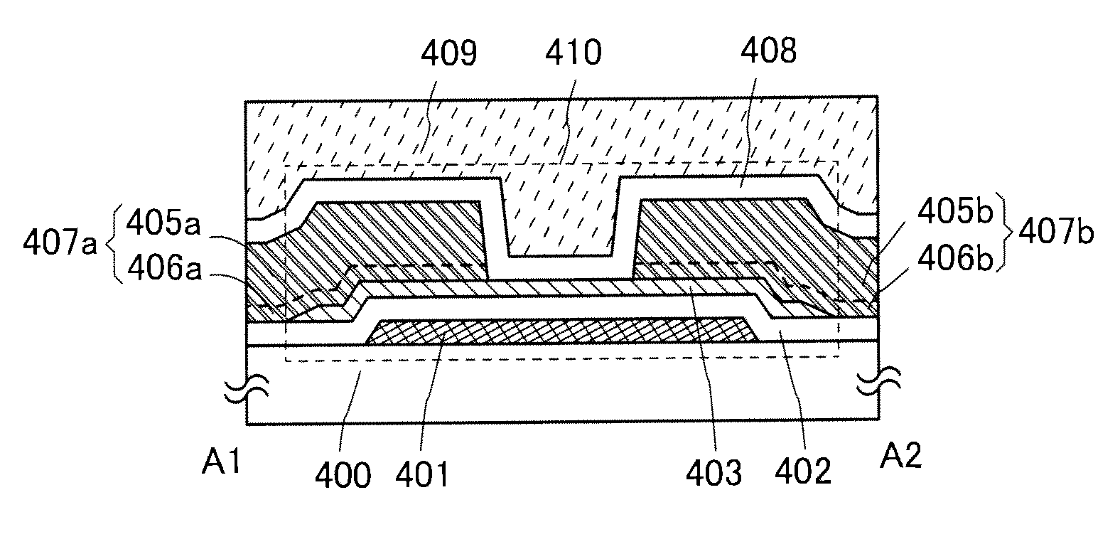
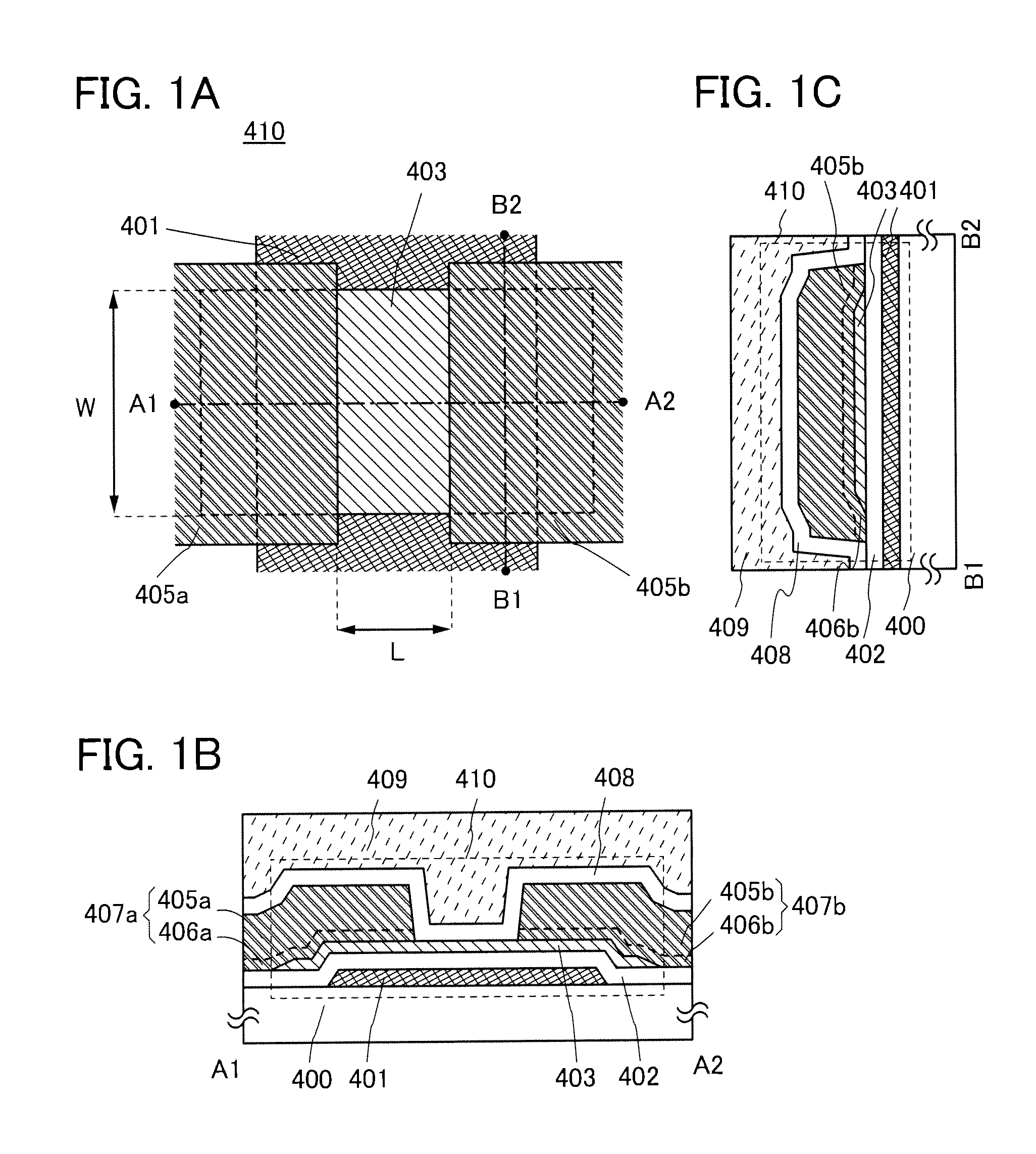
[0088]In this embodiment, one embodiment of a method for manufacturing a semiconductor device is described with reference to FIGS. 1A to 1C, FIGS. 2A and 2B, and FIG. 9. In this embodiment, a transistor including an oxide semiconductor film is described as an example of the semiconductor device.

[0089]There is no particular limitation on the structure of the transistor that can be applied to a semiconductor device according to one embodiment of the present invention; for example, a staggered type or a planar type having a top-gate structure or a bottom-gate structure can be employed. The transistor may have a single-gate structure in which one channel formation region is formed, a double-gate structure in which two channel formation regions are formed, or a triple-gate structure in which three channel formation regions are formed. Further, a transistor may have a dual-gate structure including two gate electrodes positioned above and below a channel forming region with gate insulating...

embodiment 2

[0120]In this embodiment, an example of a method for manufacturing a semiconductor device including the transistor 410 illustrated in FIGS. 1A to 1C is described with reference to FIGS. 3A to 3E.

[0121]There is no particular limitation on a substrate that can be used as the substrate 400 having an insulating surface as long as it has at least heat resistance to withstand heat treatment performed later. For example, a glass substrate of barium borosilicate glass, aluminoborosilicate glass, or the like, a ceramic substrate, a quartz substrate, or a sapphire substrate can be used. A single crystal semiconductor substrate or a polycrystalline semiconductor substrate of silicon, silicon carbide, or the like; a compound semiconductor substrate of silicon germanium or the like; an SOI substrate; or the like can be used as the substrate 400. Alternatively, any of these substrates provided with a semiconductor element may be used as the substrate 400.

[0122]The semiconductor device may be manu...

embodiment 3

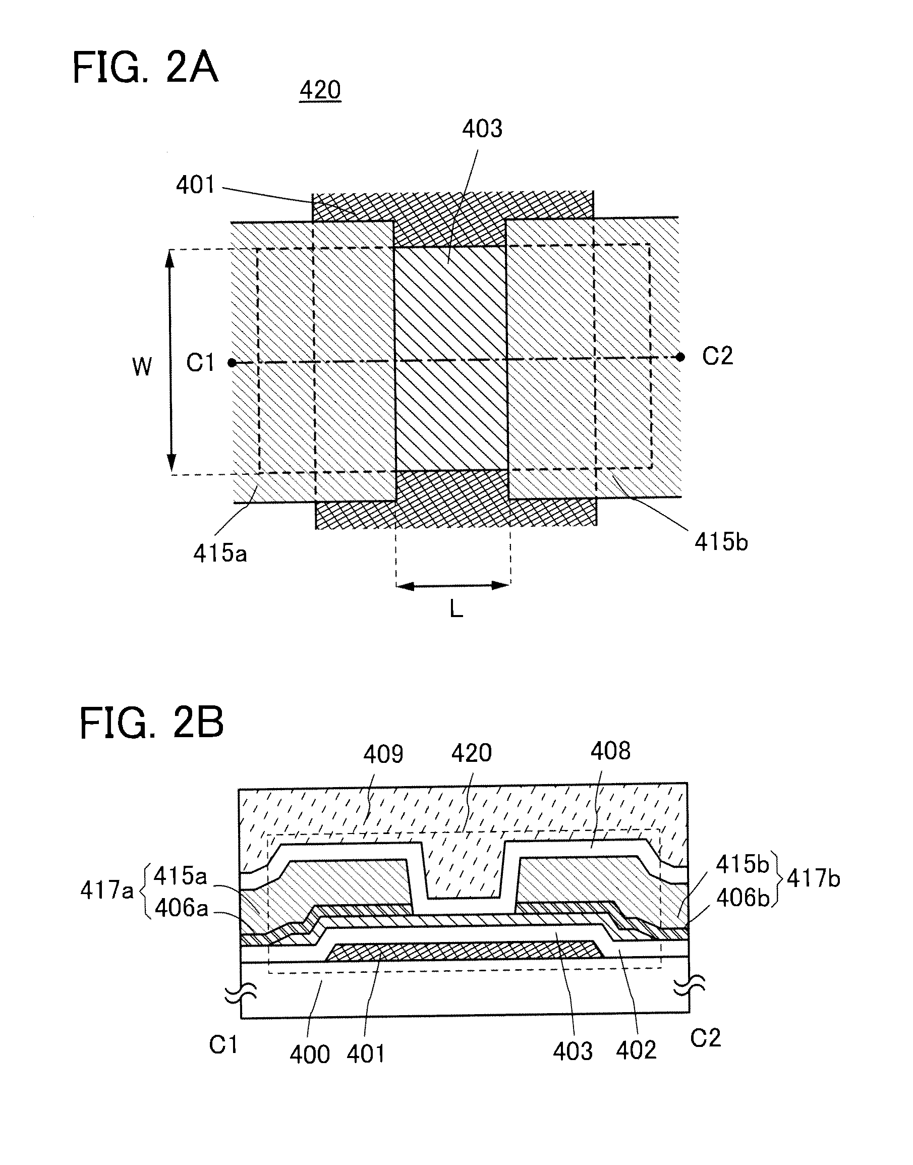
[0268]In this embodiment, another embodiment of a semiconductor device is described with reference to FIGS. 4A and 4B and FIGS. 5A and 5B. Description of the same portion as or a portion having a function similar to that in the above embodiments, a manufacturing step similar to that in the above embodiments is not repeated.

[0269]A transistor 430 illustrated in FIGS. 4A and 4B is an example of a bottom-gate transistor. FIG. 4A is a plan view of the transistor 430, and FIG. 4B is a cross-sectional view taken along line D1-D2 in FIG. 4A (a cross-sectional view in the channel length direction of the transistor 430). Further, in FIG. 4A, some components of the transistor 430 (e.g., the gate insulating film 402) are not illustrated to avoid complexity.

[0270]The transistor 430 illustrated in FIGS. 4A and 4B includes the gate electrode layer 401 over the substrate 400 having an insulating surface, the gate insulating film 402 over the gate electrode layer 401, the oxide semiconductor film 4...


PUM


Abstract

A semiconductor device in which a shift of the threshold voltage of a transistor is suppressed is provided. A semiconductor device in which a decrease in the on-state current of a transistor is suppressed is provided. The semiconductor device is manufactured as follows: forming a gate electrode layer over a substrate; forming a gate insulating film over the gate electrode layer; forming an oxide semiconductor film over the gate insulating film; forming a metal oxide film having a higher reducing property than the oxide semiconductor film over the oxide semiconductor film; performing heat treatment while the metal oxide film and the oxide semiconductor film are in contact with each other, thereby the metal oxide film is reduced so that a metal film is formed; and processing the metal film to form a source electrode layer and a drain electrode layer.

Description

BACKGROUND OF THE INVENTION[0001]1. Field of the Invention[0002]The present invention relates to a semiconductor device and a method for manufacturing the semiconductor device.[0003]In this specification, a semiconductor device generally means a device which can function by utilizing semiconductor characteristics, and an electrooptic device, a semiconductor circuit, and electronic equipment are all semiconductor devices.[0004]2. Description of the Related Art[0005]Attention has been focused on a technique for forming a transistor using a semiconductor thin film formed over a substrate having an insulating surface. The transistor is applied to a wide range of electronic devices such as an integrated circuit (IC) and an image display device (also simply referred to as display device). A silicon-based semiconductor material is widely known as a material of the semiconductor thin film applicable to the transistor. As another material, an oxide semiconductor has been attracting attention...

Claims


Application Information

Patent Timeline
IPC IPC(8): H01L29/786H01L29/66
CPCH01L29/66969H01L29/7869H01L29/45
Inventor GODO, HIROMICHI
Owner SEMICON ENERGY LAB CO LTD
Features
  • Generate Ideas
  • Intellectual Property
  • Life Sciences
  • Materials
  • Tech Scout
  • Unparalleled Data Quality
  • Higher Quality Content
  • 60% Fewer Hallucinations
Learn More