Pretreatment Method for Reduction and/or Elimination of Basal Plane Dislocations Close to Epilayer/Substrate Interface in Growth of SiC Epitaxial

a technology of epilayer and substrate, applied in the direction of crystal growth process, polycrystalline material growth, chemically reactive gas, etc., can solve the problems of reducing the practicability of the substrate etching method, reducing the defect-free region of the substrate, and reducing the device performance. , to achieve the effect of high

Inactive Publication Date: 2013-06-06
UNIVERSITY OF SOUTH CAROLINA
View PDF11 Cites 30 Cited by
  • Summary
  • Abstract
  • Description
  • Claims
  • Application Information

AI Technical Summary

Problems solved by technology

These buried BPDs may still be converted to Shockley SFs under current stress, and these SFs will extend into the drift layers and degrade the device performance.
In addition, due to the aggressive etching methods by molten KOH or regular KOH—NaOH eutectic, surface damage cannot be avoided even in the defect free regions of the substrate.
Post-polishing process is mandatory in order to obtain a smooth surface for device fabrication on the resulting epilayer, which reduces the practicability of the substrate etching method.
Another one of the greatest challenges of growing SiC epitaxial films by high temperature chemical vapor deposition (CVD) is to restrict the gas phase nucleation or cluster formation or aerosol formation of silicon during growth.
These particles adversely influence the growth by reducing the growth rate due to precursor losses and degrade the crystal quality since the Si droplets are carried to the crystal growth surface by the H2 carrier gas.
Moreover, liquid aerosol particles are viscous and adhere to the gas delivery system (parasitic deposition) and causes severe degradation of the reactor parts during epitaxial growth.
These depositions (parasitic deposition) are generally flaky, loosely bound, and can be carried to the growth surface during the growth resulting in degradation of crystal quality, introducing defects in the growing epitaxial film.
Long duration epitaxial growth to achieve thick epitaxial films is also very inconvenient using conventional Si precursors due to excessive Si cluster formation and parasitic deposition in the reactor.
Cluster formation of particles (Si) is the leading cause of yield loss in semiconductor processing and the critical particle size should be reduced as the microelectronic size decreases.
The major drawback associated with the silane chemistry in achieving high growth rates is the relatively weak bond strength of the Si—H (318 kJ / mol) bond in SiH4 causing it to dissociate easily (and very early in the gas delivery system) into elemental Si.
However, in higher temperature SiC growth (typically 1500° C. or above), dichlorosilane (SiH2Cl2) can also generate silicon droplets with increased parasitic deposition at higher gas flow rates leading to degraded epilayer surface morphology.
However, homoepitaxial growth on SiC substrates by hot wall, high temperature CVD has not been reported for high quality, thick film growth.
Moreover, it is believed in the art that SiF4 is not a suitable gas for SiC epitaxial growth due to its “too strong” Si—F bond (565 kJ / mol).

Method used


Image

  • Pretreatment Method for Reduction and/or Elimination of Basal Plane Dislocations Close to Epilayer/Substrate Interface in Growth of SiC Epitaxial
  • Pretreatment Method for Reduction and/or Elimination of Basal Plane Dislocations Close to Epilayer/Substrate Interface in Growth of SiC Epitaxial
  • Pretreatment Method for Reduction and/or Elimination of Basal Plane Dislocations Close to Epilayer/Substrate Interface in Growth of SiC Epitaxial

Examples


example 1

Fluorine Chemistry

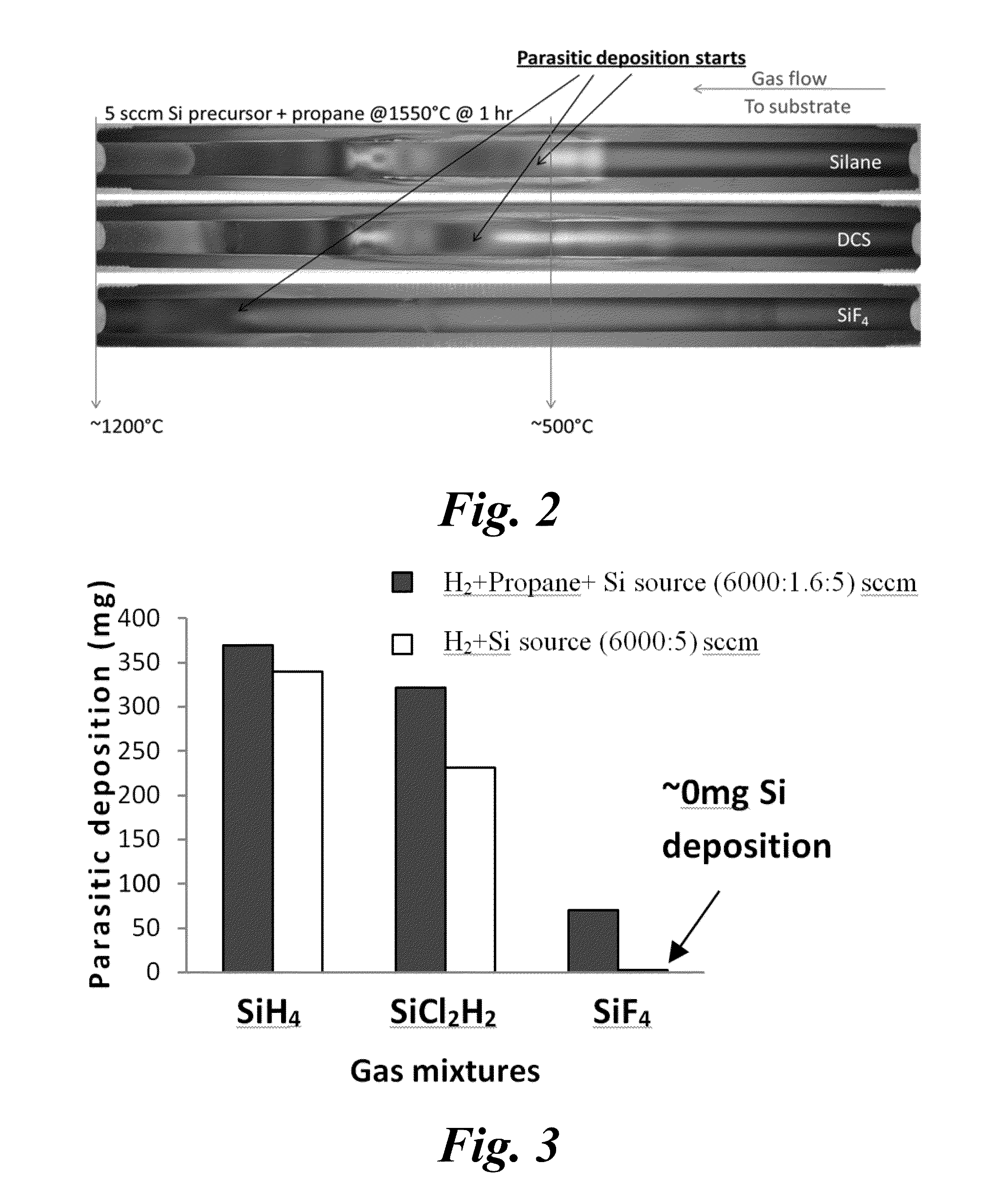
[0094]Experiments were conducted in a hot wall CVD reactor. Silicon tetrafluoride (SiF4) was used as the gas precursor for silicon source as well as conventional gases (silane and dichlorosilane) for comparisons. Propane gas was used as the carbon source, whereas hydrogen gas was used as the carrier gas. Growth temperature was kept at 1550° C. and the reactor pressure was kept fixed at 300 Torr. The C / Si ratio was maintained at 1. Commercially available 4H—SiC (Si face, 8° or 4° off cut towards [11 20] direction) substrates were used, without any surface pretreatment.

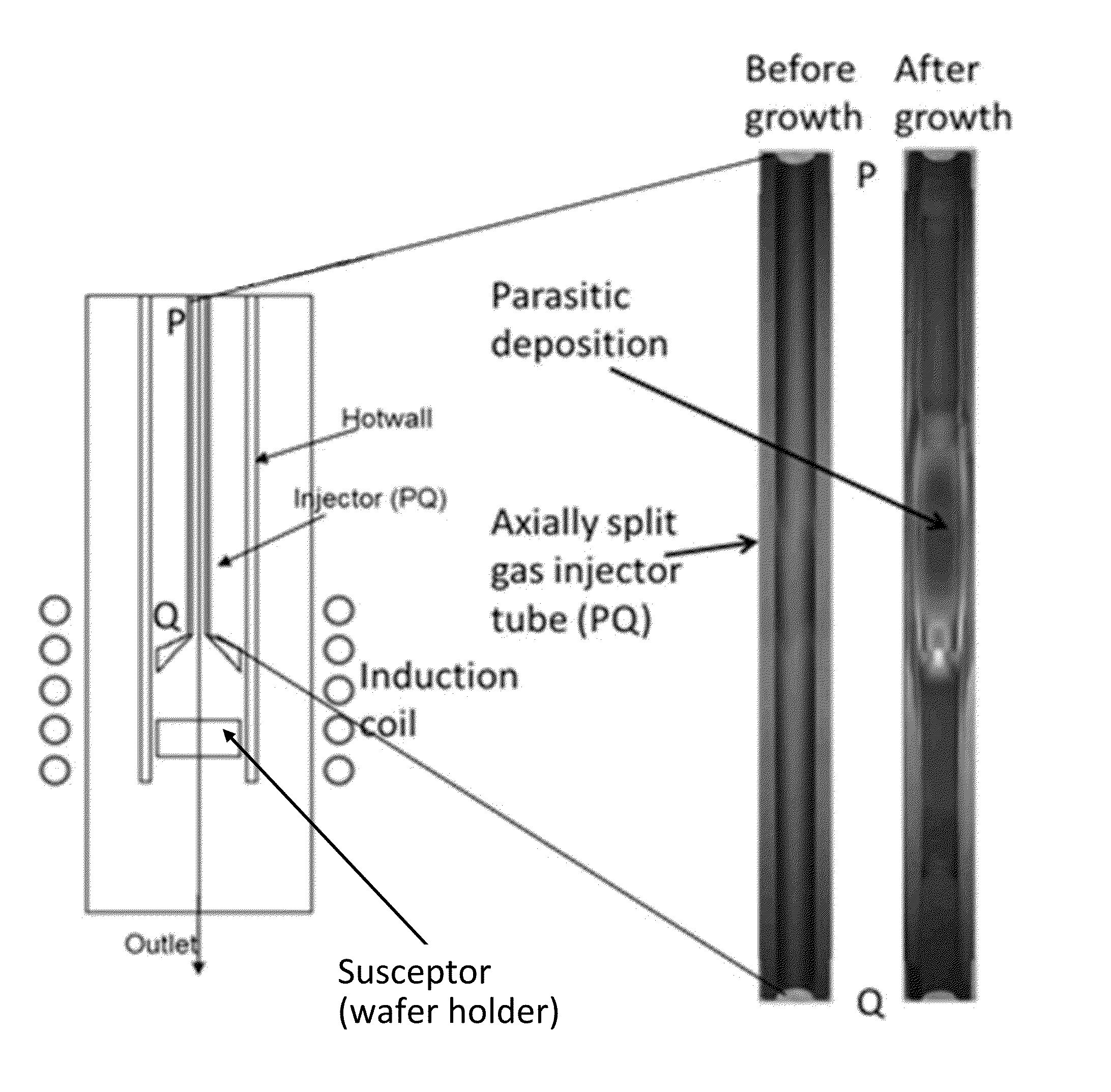
[0095]A novel gas delivery tube system (gas injector) was used to visualize the parasitic deposition in the gas delivery tube. This design was an effective tool to identify the location at which gases start decomposing in the injector tube by the observation of parasitic depositions. In this scheme, the gas delivery tube is axially split into two halves, which can be assembled together for epitaxial gr...

example 2

Substrate Surface Pretreatment

[0105]The substrate was commercially obtained 4H—SiC wafer with 8° off-axis towards [11 20] direction with the Si-face chemical mechanical polished. The substrates were treated by molten KOH-related mixture of (e.g., KOH—NaOH—MgO at 35:50:15 wt %) for different durations (2-45 min). Epitaxial growth was carried out in a home-built chimney CVD reactor at 1550° C. and 80 Torr, using propane and dichlorosilane as precursors. The doping of the epilayer is ˜1×1015 cm−3 n-type was controlled by C / Si ratio. After growth, all the samples were etched by the same etchant to delineate the defects on the epilayers.

TABLE 2Sample pretreatment condition and defect densityon the epilayers grown on 8° SiC substrates a.SubstrateEpilayerSampletreatmentEtch pit sizethicknessBPD density on theNo.durationon the substrate(μm)epilayer (cm−2)1No—61832No—61503No—62324 2 minInvisible b620512 minμm611625 min~1.5μm622745 min~4μm615  8 c 2 minInvisible b0.519a Typical BPD density on...

example 3

[0111]A fluorinated silicon precursor, silicon tetrafluoride (SiF4), was employed in SiC CVD growth to investigate the pretreatment method. The substrates are cut from a 4° off-axis 4H—SiC wafer and epitaxial growth (˜4 μm) is first carried out without any pretreatment and a surprisingly low BPD density was observed (5 cm−2) compared to the other growth method mentioned in Table 2 (sample 1, 2 and 3) using DCS as the Si precursor. Later in other experiments the surface was treated by the molten KOH-related mixture for 2 min. Epitaxial growth was then carried out using the novel SiF4 precursor described earlier on the pretreated substrate. The grown epilayer was completely BPD free, indicating that 100% BPD conversion was achieved (Table 4) at the initial stage of epigrowth (i.e., very close to the epilayer / substrate interface). This accomplishment of 100% substrate BPD conversion was accomplished from the substrate pretreatment combined with the use of the SiF4 precursor.

TABLE 4Comp...


PUM

PropertyMeasurementUnit
temperatureaaaaaaaaaa
diameteraaaaaaaaaa
temperatureaaaaaaaaaa

Abstract

Non-destructive pretreatment methods are generally provided for a surface of a SiC substrate with substantially no degradation of surface morphology thereon. In one particular embodiment, a molten mixture (e.g., including KOH and a buffering agent) is applied directly onto the surface of the SiC substrate to form a treated surface thereon. An epitaxial film (e.g., SiC) can then be grown on the treated surface to achieve very high (e.g., up to and including 100%) BPD to TED conversion rate close to the epilayer / substrate interface.

Description

PRIORITY INFORMATION[0001]The present application claims priority to U.S. Provisional Patent Application Ser. No. 61 / 716,020 titled “A Method for Elimination of Basal Plane Dislocations and In-Grown Stacking Faults with No Surface Degradation for High Quality SiC Epitaxial Films” of Sudarshan, et al. filed on Oct. 19, 2012; to U.S. Provisional Patent Application Ser. No. 61 / 638,770 titled “Method of Growing High Quality, Thick Silicon Carbide Homoepitaxial Films by Eliminating Silicon Gas Phase Nucleation and Silicon Parasitic Deposition” of Sudarshan, et al. filed on Apr. 26, 2012; and to U.S. Provisional Patent Application Ser. No. 61 / 563,250 titled “Substrate Pretreatment Method for Reduction / Elimination of Basal Plane Dislocations and In-Grown Stacking Faults with No Surface Degradation for High Quality SiC Epitaxial Films” of Sudarshan, et al. filed on Nov. 23, 2011. The disclosures of all of these priority applications are incorporated by reference herein.GOVERNMENT SUPPORT CL...

Claims


Application Information

Patent Timeline
Patent Type & Authority Applications(United States)
IPC IPC(8): H01L21/02
CPCH01L21/02658H01L21/02082H01L21/02516H01L21/02529H01L21/0262H01L21/30608C30B25/20C30B25/14C30B25/165C30B29/36C30B25/183C30B25/186H01L21/02019H01L21/02433H01L21/02378H01L21/02447H01L29/1608
Inventor SUDARSHAN, TANGALI S.SONG, HAIZHENGRANA, TAWHID
Owner UNIVERSITY OF SOUTH CAROLINA
Why Eureka
Try Eureka