Nitride semiconductor template and light-emitting diode

a semiconductor and template technology, applied in semiconductor/solid-state device manufacturing, semiconductor devices, electrical devices, etc., can solve the problems of reducing reliability, reducing reliability, and reducing brightness of light-emitting diodes, and achieves low resistance, good crystalline characteristics, and low resistance.

Active Publication Date: 2013-06-20
SUMITOMO CHEM CO LTD
View PDF13 Cites 7 Cited by
  • Summary
  • Abstract
  • Description
  • Claims
  • Application Information

AI Technical Summary

Benefits of technology

[0045]According to one embodiment of the invention, where a substrate (PSS substrate) with convex portions formed on a surface thereof is used as a substrate, it is possible to provide a nitride semiconductor template having low resistance (surface resistivity of not more than 30 Ω / sq) and good crystalline characteristics (XRD half-value width of not less than 50 seconds and not more than 100 seconds), and a light-emitting diode using thereof. In addition, in case of using a planar substrate not having convex portions on a surface thereof (a substrate other than the PSS substrate), it is possible to provide a nitride semiconductor template having low resistance (surface resistivity of not more than 30 Ω / sq) and good crystalline characteristics (XRD half-value width of not less than 50 seconds and not more than 300 seconds), and a light-emitting diode using thereof.

Problems solved by technology

However, increasing the amount of impurity added to the uppermost layer deteriorates crystalline characteristics, which results in a decrease in brightness of the light-emitting diode.
In addition, when the impurity amount is large, brightness is reduced due to dopant diffusion into a light-emitting portion, especially into an active layer, formed on the template and reliability decreases due to the dopant diffusion.
If the impurity is increased to increase the carrier concentration, the impurity in the nitride semiconductor template is diffused into the light-emitting layer during growth of the light-emitting layer portion by the MOVPE method performed later on, which decreases reliability as LED.

Method used


Image

  • Nitride semiconductor template and light-emitting diode
  • Nitride semiconductor template and light-emitting diode
  • Nitride semiconductor template and light-emitting diode

Examples


first embodiment

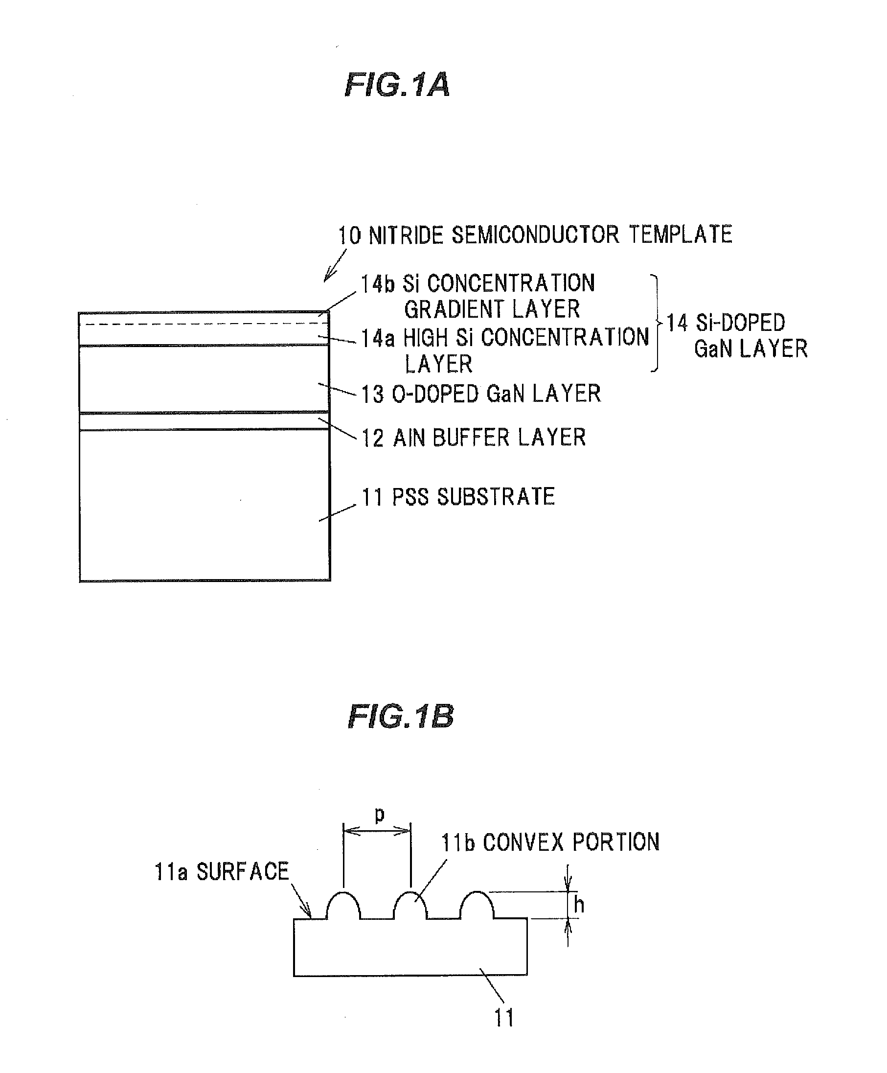
[0063]FIG. 1A is a cross sectional view showing a nitride semiconductor template in a first embodiment of the invention and FIG. 1B is a principal-portion cross sectional view showing a surface state of a substrate.

[0064]A nitride semiconductor template 10 has a sapphire substrate with a patterned surface, i.e., a PSS (Patterned Sapphire Substrate) 11, and an AlN buffer layer 12 as a buffer layer formed on the PSS substrate 11, an O-doped GaN layer 13 as a first layer which is an O-doped layer doped with O (oxygen) and is formed on the AlN buffer layer 12, and a Si-doped GaN layer 14 as a second layer (the uppermost layer) which is a Si-doped layer doped with silicon (Si) and is formed on the O-doped GaN layer 13.

[0065]The Si-doped GaN layer 14 is provided with a high Si concentration layer 14a having a region in which a carrier concentration is uniform in a thickness direction, and a Si concentration gradient layer 14b having a carrier concentration which gradually decreases from t...

second embodiment

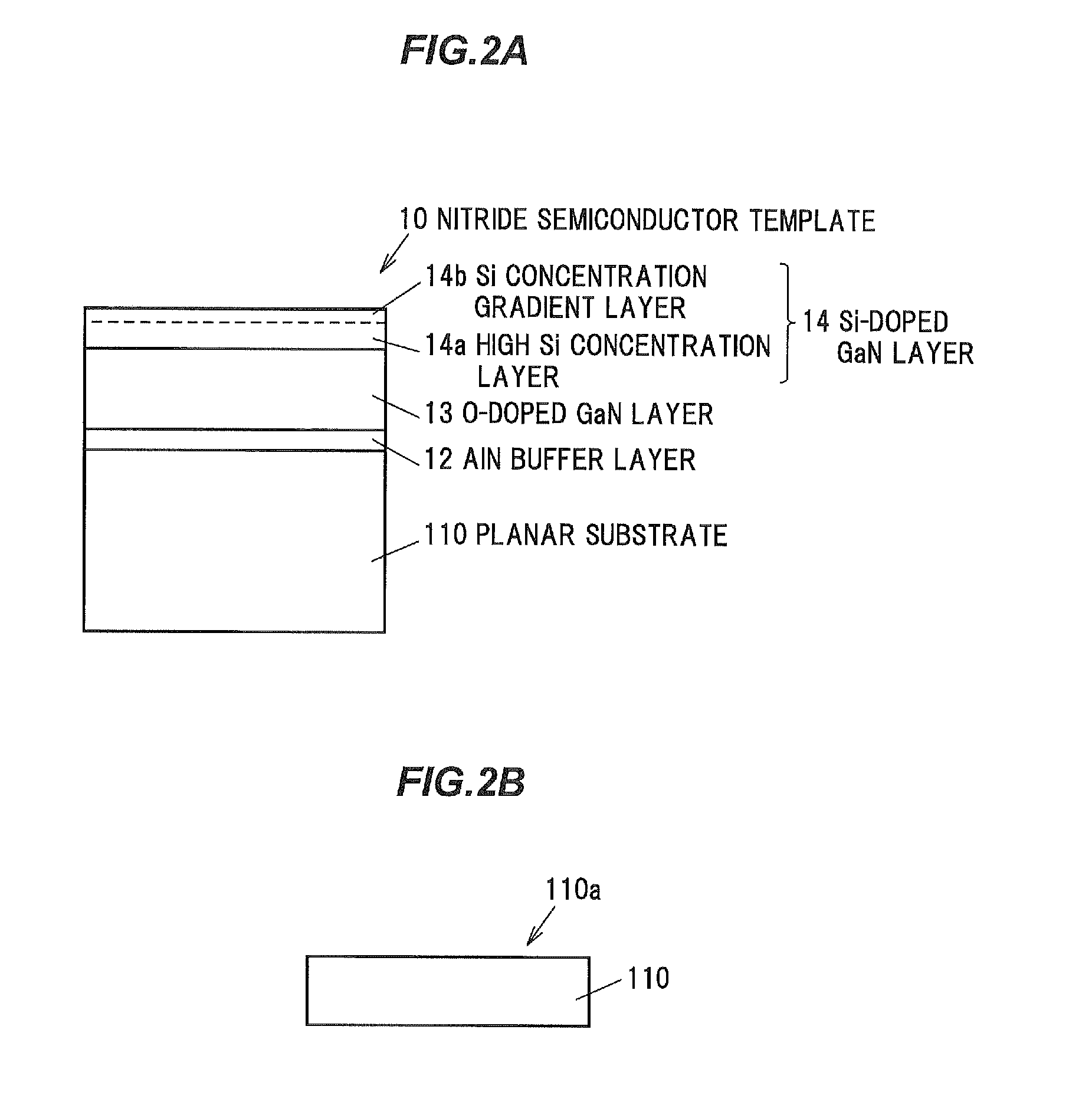
[0096]FIG. 2A is a cross sectional view showing a nitride semiconductor template in a second embodiment of the invention. It is basically the same as the cross sectional view of the nitride semiconductor template in the first embodiment of the invention shown in FIG. 1A. FIG. 2B is a principal-portion cross sectional view showing a surface state of a substrate. The second embodiment is different from the first embodiment in that a planar substrate 110 which is flat without having convex portions 11b on a surface 110a is used as a substrate. For example, a sapphire substrate is used as the planar substrate 110.

third embodiment

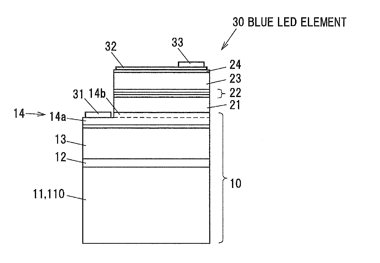
[0097]FIG. 3 is a cross sectional view showing a light-emitting diode epitaxial wafer in a third embodiment of the invention. In a light-emitting diode epitaxial wafer 20 in the third embodiment, an n-type GaN layer 21 is grown on the nitride semiconductor template 10 shown in FIG. 1 or 2, six pairs of InGaN / GaN multiple quantum well layers 22 are grown thereon, and a p-type AlGaN layer 23 and a p-type GaN contact layer 24 are grown thereon. The structures shown in FIGS. 1 and 2 here are examples of the nitride semiconductor template. The n-type GaN layer 21 is an example of the n-type nitride semiconductor layer. The p-type AlGaN layer 23 and the p-type GaN contact layer 24 are examples of a p-type nitride semiconductor layer.


PUM

PropertyMeasurementUnit
thicknessaaaaaaaaaa
thicknessaaaaaaaaaa
carrier concentrationaaaaaaaaaa

Abstract

A nitride semiconductor template includes a substrate, and a group III nitride semiconductor layer formed on the substrate and including a Si-doped layer doped with Si as an uppermost layer thereof. The group III nitride semiconductor layer has a total thickness of not less than 4 μm and not more than 10 μm. The Si-doped layer includes a Si concentration gradient layer having a carrier concentration that gradually decreases toward an outermost surface thereof so as to be not less than 1×1017 cm−3 and not more than 5×1017 cm−3 at the outermost surface of the group III nitride semiconductor layer.

Description

[0001]The present application is based on Japanese patent application Nos. 2011-274222 and 2012-250072 filed on Dec. 15, 2011 and Nov. 14, 2012, respectively, the entire contents of which are incorporated herein by reference.BACKGROUND OF THE INVENTION[0002]1. Field of the Invention[0003]The invention relates to a nitride semiconductor template and a light-emitting diode using the nitride semiconductor template.[0004]2. Description of the Related Art[0005]Nitride-based compound semiconductors such as gallium nitride (GaN), aluminum gallium nitride (AlGaN) and indium gallium nitride (InGaN) have received attention as a light-emitting element material capable of emitting light from red to ultraviolet. One of crystal growth methods of such nitride semiconductor materials is a Hydride Vapor Phase Epitaxy (HVPE) method in which metal chloride gas and ammonia are used as raw materials.[0006]The HVPE method is characterized in that it is possible to obtain a growth rate of not less than 10...

Claims


Application Information

Patent Timeline
Patent Type & Authority Applications(United States)
IPC IPC(8): H01L29/36H01L33/06
CPCH01L29/36H01L33/06H01L33/025H01L33/325H01L21/0242H01L21/0243H01L21/02458H01L21/02502H01L21/0254H01L21/02573H01L21/02576H01L21/0262
Inventor KONNO, TAICHIROOFUJIKURA, HAJIME
Owner SUMITOMO CHEM CO LTD
Why Eureka
Try Eureka