Printed Temperature Sensor

a temperature sensor and printed technology, applied in thermoelectric device manufacture/treatment, instruments, heat measurement, etc., can solve the problems of not being compliant with modern legislation, limiting the use of substrate materials, so as to achieve low aspect ratio of thermistor devices and high resistivity of printed silicon materials.

Inactive Publication Date: 2013-08-08
PST SENSORS
View PDF4 Cites 31 Cited by
  • Summary
  • Abstract
  • Description
  • Claims
  • Application Information

AI Technical Summary

Benefits of technology

[0032]The method may include the addition of at least one additional conducting path into the silicon particle layer by the modification of the ink composition, by varying the silicon to binder ratio, or the addition of either an insulating phase such as silica or other ceramic nanoparticles, or a conducting or semiconducting phase to the ink, thereby effectively to add a relatively temperature independent internal resistance in parallel with the temperature dependent resistance of the thermistor structure.
[0033]The addition of extra conducting paths into the silicon particle layer has the effect of adding a relatively temperature independent internal resistance in parallel with the temperature dependent material of the thermistor structure. This combination may also be used to modify the temperature sensitivity of the device.
[0036]Similarly the nominal resistance of the printed temperature sensor can be increased by printing a temperature independent internal resistance in series with the temperature dependent resistance of the thermistor structure.
[0048]In one preferred embodiment, the contacts have a circular geometry so that the radial electrical path of the thermistor structure ensures that the resistance measured is averaged over all directions relative to the printing direction, thus eliminating the effect of any lateral anisotropy in the printing process.

Problems solved by technology

Invariably, because of distortion during the thermal treatment, further trimming of the material to obtain the correct resistance is required before metallization, in the case of thick-film thermistors.
The fabrication processes used place limitations on the substrate materials that can be used, precluding the use of many lightweight, flexible materials such as paper and polymer film.
Traditionally, thick-film inks used for the fabrication of thermistors are composed of heavy metal sulphides and or tellurides, such as lead sulphide, and are not compliant with modern legislation such as the European Restriction on Hazardous Substances (ROHS).

Method used


Image

  • Printed Temperature Sensor
  • Printed Temperature Sensor
  • Printed Temperature Sensor

Examples


example 1

[0090]In a first example a negative temperature coefficient thermistor was produced according to the design shown in FIG. 6. Four silver electrodes or contacts were deposited on 80 g / m2 wood-free paper sheet substrate by screen-printing using Du Pont 5000 silver conductor. The separation between any two adjacent electrodes was 2 mm. After allowing the silver ink to dry for approximately one day under ambient conditions, silicon ink was drop-cast to form a connection between all four electrodes of the device. The silicon nanoparticles used in the ink were milled from a boron doped p-type silicon wafer, according to the method disclosed in WO 2009 / 125370. These particles were mixed with a commercially available acrylic screen-printing base in a ratio of 95% silicon by weight, and the consistency of the ink was adjusted by thinning with propylene glycol.

[0091]The completed device was cut out from the larger sheet of paper to form a small flexible device of size approximately 15 mm by 1...

example 2

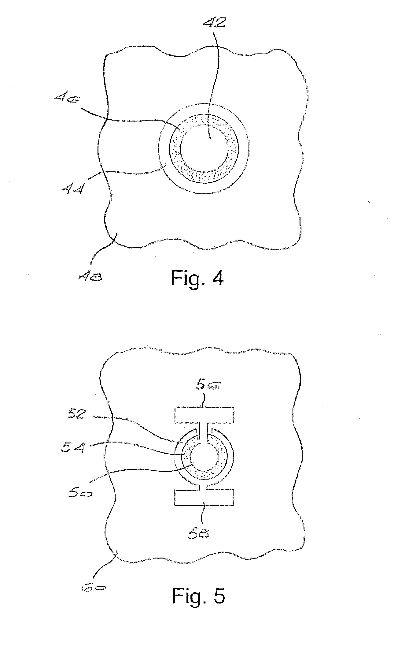
[0094]In a second example a negative temperature coefficient thermistor was produced, also according to the design shown in FIG. 5. Silver contacts were deposited on a substrate comprising a sheet of 80 g / m2 wood-free paper by screen-printing using Du Pont 5000 silver conductor. The diameter of the inner electrode was 5 mm, and the separation between the two electrodes was 0.5 mm. After allowing the silver ink to dry for approximately one day under ambient conditions, a silicon layer was screen-printed over the gap between the electrodes, using silicon nanoparticles milled from 2503 grade metallurgical silicon according to the method disclosed in WO 2009 / 125370. These nanoparticles were mixed with a commercially available acrylic screen-printing base in a ratio of 88% silicon by weight, and the consistency of the ink was adjusted by thinning with propylene glycol.

[0095]The completed device was cut out from the larger sheet of paper to form a small flexible device of size approximate...

example 3

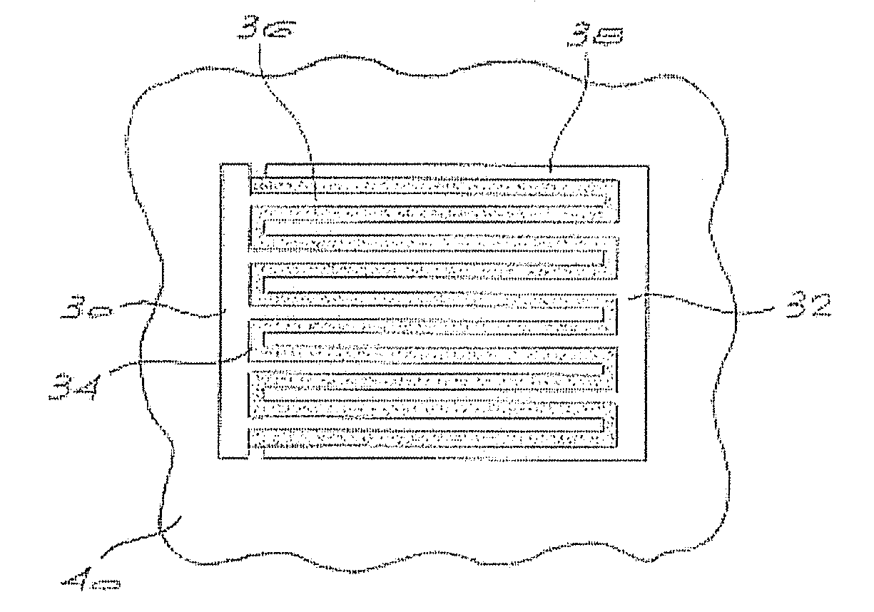
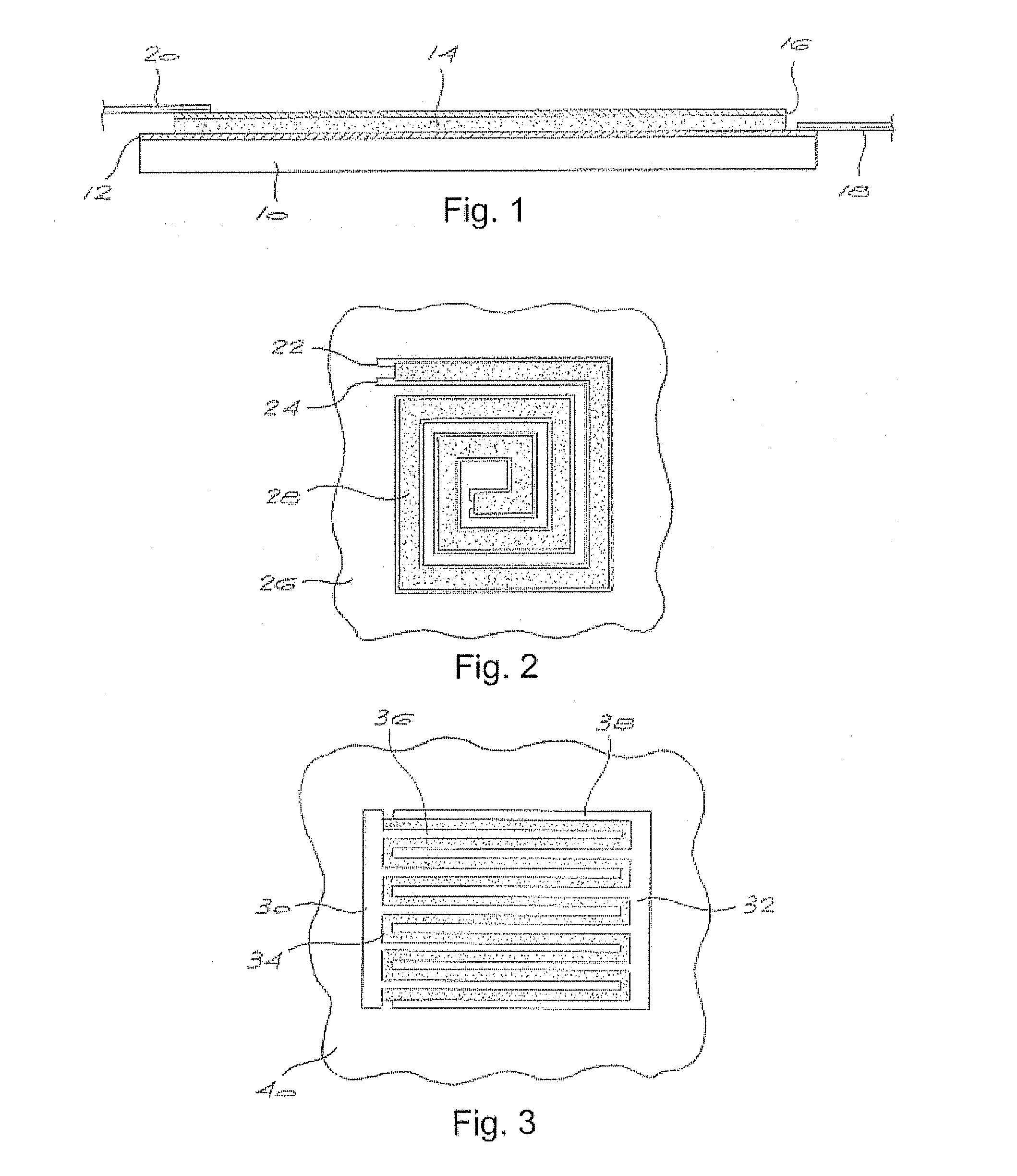
[0096]FIG. 11 is a photograph of a negative temperature coefficient thermistor according to the design shown in FIG. 3. In this case the silicon is printed as a solid block over the interdigitated silver contacts, but only the area of silicon deposited between the contacts contributes to the temperature dependent resistance. For a low resistance, the length to width aspect ratio of the silicon semiconductor should be low, ideally less than 1 / 1 000. In this example, the silver contacts comprise 25 individual electrodes, with 24 gaps between adjacent electrodes, each gap having a length of 16 mm and the width of each gap (the separation between adjacent electrodes) of 0.25 mm.

[0097]In contrast to the device of Example 2, which is a high resistance device and has a length to width aspect ratio of approximately 1 / 30 (given by the ratio of the transverse gap between the conductors to the circumference of a circle defining the gap between the conductors in FIG. 5), the design of the prese...


PUM

PropertyMeasurementUnit
sizeaaaaaaaaaa
sizeaaaaaaaaaa
sizeaaaaaaaaaa

Abstract

A method of producing a temperature sensing device is provided. The method includes forming at least one silicon layer and at least one electrode or contact to define a thermistor structure. At least the silicon layer is formed by printing, and at least one of the silicon layer and the electrode or contact is supported by a substrate during printing thereof. Preferably, the electrodes or contacts are formed by printing, using an ink comprising silicon particles having a size in the range 10 nanometres to 100 micrometres, and a liquid vehicle composed of a binder and a suitable solvent. In some embodiments the substrate is an object the temperature of which is to be measured. Instead, the substrate may be a template, may be sacrificial, or may be a flexible or rigid material. Various device geometries are disclosed.

Description

BACKGROUND OF THE INVENTION[0001]THIS invention relates to a temperature sensing device and a method of producing such devices. In particular the invention relates to a negative temperature coefficient thermistor.[0002]Printing of functional inks has a long tradition in the electronics field. For example, pigment based inks are used to screen-print interconnections and resistors on printed circuit boards. In these applications the thick film inks used consist of a vehicle and pigments of silver and carbon respectively, where the pigment particles can have a dimension in the nanometer range.[0003]Traditionally most functional materials have been printed by conventional printing techniques, such as screen printing. More recent developments are aimed at printing not only the passive components of a circuit, but also active components. For example, printed nanoparticulate silicon components are disclosed in International patent application WO 2004 / 068536, which discloses the printing of...

Claims


Application Information

Patent Timeline
Patent Type & Authority Applications(United States)
IPC IPC(8): H01L35/34
CPCH01C7/041G01K7/226H01L35/34H01C17/06H01C7/04G01K7/22H05K3/12H01C7/02H05K1/16H10N10/01
Inventor BRITTON, DAVID THOMASHARTING, MARGIT
Owner PST SENSORS
Why Eureka
Try Eureka