Supercharge Your Innovation With Domain-Expert AI Agents!

Perovskite oxide film and ferroelectric film using the same, ferroelectric device, and method for manufacturing perovskite oxide film

Active Publication Date: 2013-09-12
FUJIFILM CORP +1
View PDF4 Cites 9 Cited by
  • Summary
  • Abstract
  • Description
  • Claims
  • Application Information

AI Technical Summary

Benefits of technology

The present invention provides a method for forming a potassium niobate mixed crystal perovskite oxide film with good crystallinity and minimal defects, such as cracks. The method involves low-temperature film formation using hydrothermal synthesis and careful consideration of factors that affect the composition of the film. The resulting film has a stable composition and is useful in a variety of applications.

Problems solved by technology

1646-1649, 2009, the composition control for the mixed crystal of potassium niobate is extremely difficult, whereby it is difficult to obtain a single crystal of good crystallinity.

Method used


Image

  • Perovskite oxide film and ferroelectric film using the same, ferroelectric device, and method for manufacturing perovskite oxide film
  • Perovskite oxide film and ferroelectric film using the same, ferroelectric device, and method for manufacturing perovskite oxide film
  • Perovskite oxide film and ferroelectric film using the same, ferroelectric device, and method for manufacturing perovskite oxide film

Examples


example 1

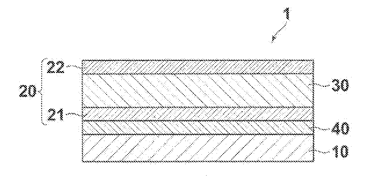
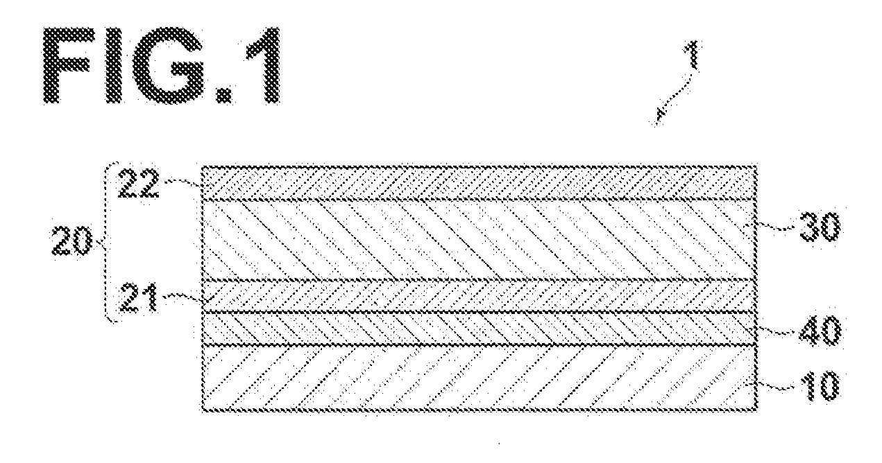
[0091]A (100) SrTiO3 (STO) substrate with a thickness of 500 μm was prepared and a SrRuO3 (SRO) back contact electrode was formed on the surface of the substrate with a thickness of about 60 nm by sputtering. In forming the electrode, a commercially available SRO target was used as the target under the following film forming conditions: output power of 60 W; substrate temperature of about 600° C.; deposition pressure of 27 Pa; argon-oxygen ratio of 20 / 5; substrate-target distance of 120 mm; and deposition time of about 220 minutes.

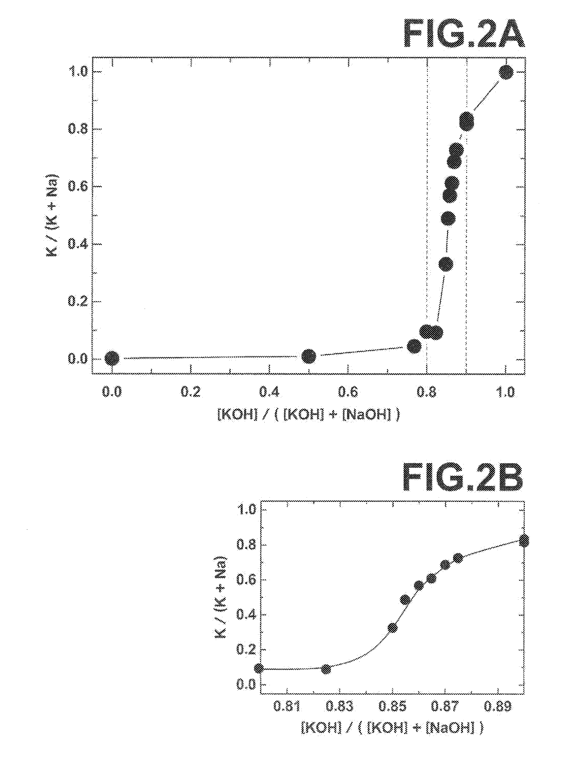
[0092]Then, reaction solutions were prepared. 9×10⁻⁴ mol of Nb2O5 powder, 7 mol / l of KOH, and 7 mol / l of NaOH were provided and mixed to prepare for a 20 ml of reaction solution having each of the predetermined compositions shown in Table 1.

[0093]Each reaction solution shown in Table 1 was put into a temperature controllable reaction vessel and the temperature was controlled such that the temperature of each reaction solution becomes 240° C. Then the subst...

example 2

[0099]As the substrate, following three substrates were provided.[0100]1> inconel substrate (300 μm thickness)[0101]2> SrRuO3 (SRO) / inconel substrate (300 μm thickness)

[0102]Film forming conditions: A SrRuO3 (SRO) was formed on a 300 μm thick inconel substrate by sputtering with a thickness of about 120 nm as a buffer layer. A commercially available SRO target was used as the target, Film forming conditions: output power of 40 W; substrate temperature of about 600° C.; deposition pressure of 8 Pa; argon-oxygen ratio of 70 / 30; substrate-target distance of 70 mm; and deposition time of about 60 minutes.[0103]3> SRO / La2NiO4 (LNO) / inconel substrate (300 μm thickness)

[0104]Film forming conditions: A SRO (film thickness of about 120 nm) / La2NiO4 (LNO) (film thickness of about 150) was formed on a 300 μm thick inconel substrate by sputtering as a buffer layer. A commercially available SRO and LNO targets were used as the targets. With respect to the LNO, film forming was performed under thr...

example 3

[0113]A 300 μm thick inconel substrate formed in a cantilever shape by wire electrical discharge machining was provided and SrRuO3(SRO) was formed on the surface thereof with a thickness of about 120 nm as a buffer layer. The film forming conditions were similar to those of the substrate 2 in Example 2.

[0114]Then, a 20 ml of reaction solution having the same composition as that of No. 12 in Table 1 was prepared, and a (K, Na)NbO3 film was formed on the SRO buffer layer with a thickness of about 6 μm as in each substrate in Example 2. The results of composition analysis performed in the same manner as in Example 1 showed that the composition of K / (K+Na) in the film was 0.88.

[0115]Next, an Au upper electrode was provided on the (K, Na)NbO3 film by low vacuum vapor deposition, thereby providing a measuring sample (cantilever) for piezoelectric property evaluation. Note that the sample was not subjected to polarization treatment. The piezoelectric property evaluation was performed by a ...


PUM

PropertyMeasurementUnit
Temperatureaaaaaaaaaa
Lattice constantaaaaaaaaaa
Thicknessaaaaaaaaaa

Abstract

A perovskite oxide film is formed on a substrate, in which the perovskite oxide film has an average film thickness of not less than 5 μm and includes a perovskite oxide represented by a general formula (P) given below:(K1−w−x, Aw, Bx)(Nb1−y−z, Cy, Dz)O3 - - - (P),where: 0<w<1.0, 0≦x≦0.2, 0≦y<1.0, 0≦z≦0.2, 0<w+x<1.0, A is an A-site element having an ionic valence of 1 other than K, B is an A-site element, C is a B-site element having an ionic valence of 5, D is a B-site element, each of A to D is one kind or a plurality of kinds of metal elements.

Description

TECHNICAL FIELD[0001]The present invention relates to an I-V perovskite oxide film and ferroelectric film using the same, a ferroelectric device, and a method for manufacturing the I-V perovskite oxide film.BACKGROUND ART[0002]Today, with an increasing interest in the environmental impact, switching to a non-lead based system has been actively conducted for piezoelectric films used for piezoelectric actuators, ultrasound probes, pressure sensors, and the like. As one of non-lead perovskite oxides expected to have high piezoelectric and ferroelectric performance, a I-V perovskite oxide in which A-site element includes a monovalent metal element (K, Na, Li, or the like) and B-site element includes a pentavalent metal element (Nb, Ta, Sb, or the like) has been studied.[0003]Among I-V perovskite oxides expected to have high piezoelectricity and ferroelectricity, a potassium niobate (KNbO3) (hereinafter, KN) perovskite oxides is known as having a high electromechanical coupling coefficie...

Claims


Application Information

Patent Timeline
IPC IPC(8): H01L41/187H01L41/18H01L41/317B41J2/14B41J2/16C01G33/00H01L21/208H01L21/8246H01L27/105H01L41/08H01L41/09H01L41/22H01L41/39
CPCC23C4/105C23C26/00C23C30/00H01L21/02197H01L41/1873H01L41/18Y10T428/26C23C28/042C23C28/322C23C28/3455H01L21/02282H01L21/02304Y10T428/269H01L41/317C23C4/11H10N30/8542H10N30/077H10N30/708H10N30/85
Inventor SAKASHITA, YUKIOFUNAKUBO, HIROSHIKUROSAWA, MINORUISHIKAWA, MUTSUOEINISHI, HIROSHIRAISHI, TAKAHISA
Owner FUJIFILM CORP
Features
  • R&D
  • Intellectual Property
  • Life Sciences
  • Materials
  • Tech Scout
  • Unparalleled Data Quality
  • Higher Quality Content
  • 60% Fewer Hallucinations
Learn More