Method of Separating Surface Layer of Semiconductor Crystal Using a Laser Beam Perpendicular to the Separating Plane

a laser beam and semiconductor crystal technology, applied in the direction of polycrystalline material growth, after-treatment details, manufacturing tools, etc., can solve the problems of overdeposition of evaporated material additional consumption of expensive semiconductor materials, microcracks on the cut edges, etc., to achieve the reduction of the mechanical strength of the crystal in the separation plane with the set of local regions

Active Publication Date: 2013-09-26
SHRETER YURY GEORGIEVICH +2
View PDF10 Cites 31 Cited by
  • Summary
  • Abstract
  • Description
  • Claims
  • Application Information

AI Technical Summary

Benefits of technology

[0016]In this case, movement of the laser beam focus in the horizontal plane parallel to the crystal surface through which laser beam enters the crystal, and perpendicular to the axis of the focused laser beam cone, leads to creation of a set of the non-overlapping local regions with disturbed structure of the chemical bonds in the layer separation plane which is placed under the separable surface of the crystal in the depth defined by the depth of laser beam focusing. Since mechanical strength of the crystal in the separation plane with the set of the local regions is significantly reduced, then in applying external mechanical or thermomechanical stress, crystal splits along this plane with separating the surface layer lying higher or lower the separation plane depending on the depth of the laser beam focusing.
[0017]Separation method according to the second variation allows cutting the semiconductor crystals and boules laterally separating the surface layers from the semiconductor crystals, semiconductor washers from cylindrical semiconductor boules without loss of semiconductor material. In application to semiconductor crystals and cylindrical semiconductor boules with grown surface instrument structures, the second variation of the method allows separating thin semiconductor layers and thin semiconductor washers with grown surface instrument structures from semiconductor crystals and cylindrical semiconductor boules respectively.

Problems solved by technology

The drawback of the cutting method with the beam focusing onto the crystal surface is overdeposition of the part of the evaporated material on the cut edges, and microcracks on the cut edges, caused by thermal stresses (U.S. Pat. No. 7,682,937).
This leads to an additional consumption of the expensive semiconductor material and in the necessity of removing the overdeposited material by means of chemical etching as described in patents U.S. Pat. No. 4,224,101, U.S. Pat. No. 7,682,937.
The above methods of vertical laser cutting allow cutting the semiconductor crystals 101, FIG. 1 and FIG. 2, and semiconductor washers into separate chips, but not able to provide separation of the semiconductor instrument structures from the crystal substrates in horizontal plane or semiconductor washers from cylindrical semiconductor boules.

Method used


Image

  • Method of Separating Surface Layer of Semiconductor Crystal Using a Laser Beam Perpendicular to the Separating Plane
  • Method of Separating Surface Layer of Semiconductor Crystal Using a Laser Beam Perpendicular to the Separating Plane
  • Method of Separating Surface Layer of Semiconductor Crystal Using a Laser Beam Perpendicular to the Separating Plane

Examples


example 1

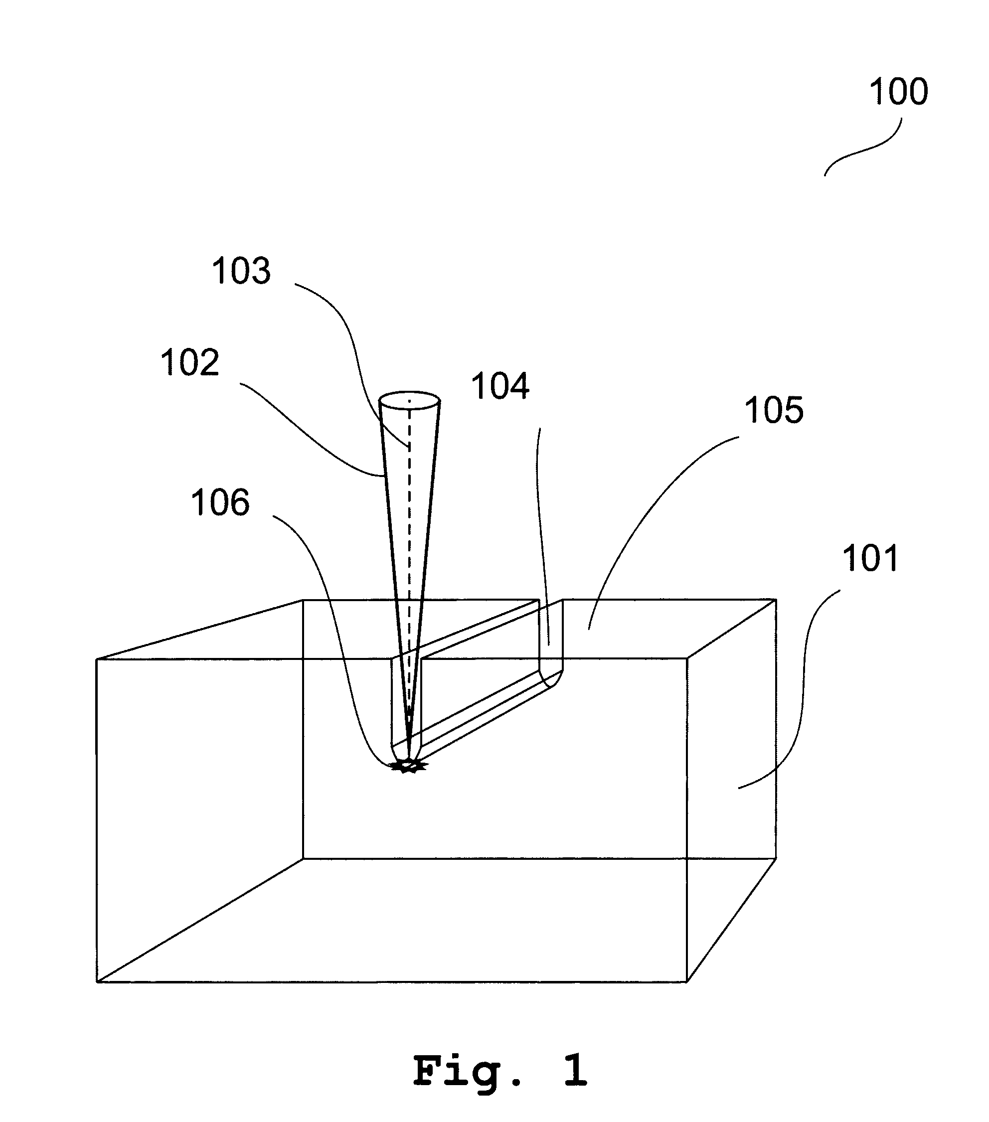
[0038]FIG. 3 shows the scheme 300 illustrating the first variation of the method by the example of separating the surface layer of the gallium nitride semiconductor crystal. For this purpose Nd:YAG laser is used which operates in the mode of modulated Q-factor, with frequency doubling and generates light pulses with λ=532 nm, energy of 5 μJ, duration of 5 ns and repetition rate of 1000 Hz. Laser beam is focused to the spot of 16 μm in diameter which provides energy density of 2 J / cm2.

[0039]Under action of the Nd:YAG laser beam 102 with wavelength λ=532 nm weakly absorbed in the gallium nitride crystal 101, focused under the upper crystal surface 105 at the depth of 100 μm, the crystal is locally heated up to temperature higher than 900° C. leading to chemical decomposition of gallium nitride crystal into gaseous nitrogen and liquid gallium in the vicinity 106 of the laser beam focus. Movement of the laser beam 102 focus at velocity of 1.5 cm / s in the horizontal (lateral) plane paral...

example 2

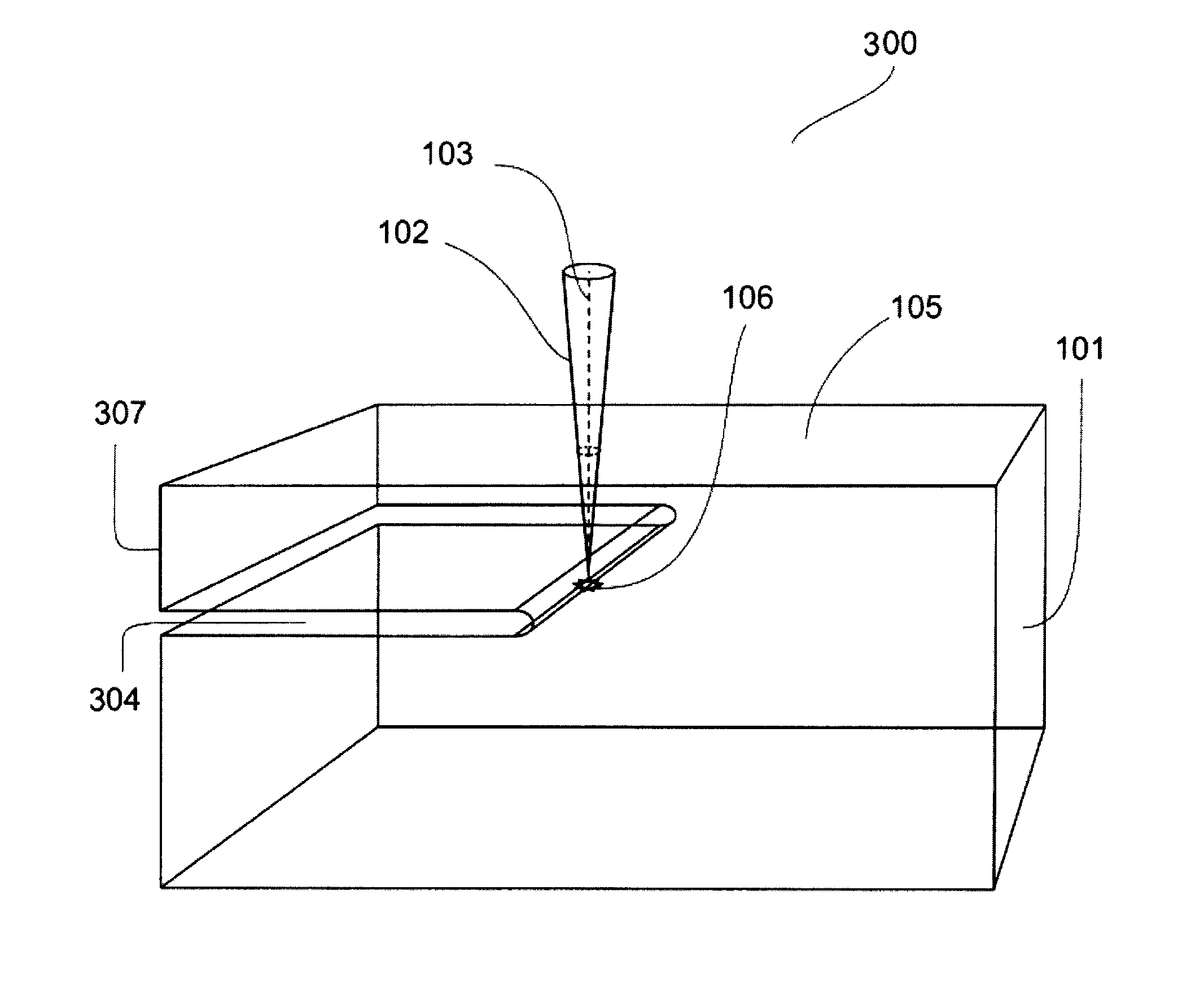
[0040]FIG. 4 shows the scheme 400 illustrating the first variation of the method by the example of separating a thin semiconductor layer comprising a grown light diode structure AlGaN / InGaN / AlGaN under the upper surface, from semiconductor crystal. For this purpose Nd:YAG laser is used which operates in the mode of modulated Q-factor, and generates light pulses with λ=532 nm, energy of 5 μJ, duration of 5 ns and repetition rate of 1000 Hz. Laser beam is focused to the spot of 16 μm in diameter which provides energy density of 2 J / cm2.

[0041]Under action of the Nd:YAG laser emission 102 with wavelengthλ=532 nm weakly absorbed in the gallium nitride crystal 101 and in the light diode structure 407 AlGaN / InGaN / AlGaN, focused under the surface 105 at the depth of 50 μm, the crystal is locally heated up to temperature higher than 900° C. leading to chemical decomposition of gallium nitride crystal into gaseous nitrogen and liquid gallium in the vicinity 106 of the laser beam focus. Moveme...

example 3

[0042]FIG. 5 is a scheme 500 illustrating the first variation of the method by the example of separating a thin semiconductor layer comprising a grown light diode structure AlGaN / InGaN / AlGaN in the base, from semiconductor crystal.

[0043]For this purpose Nd:YAG laser is used which operates in the mode of modulated Q-factor at λ=532 nm, and generates pulses with energy of 5 μJ, duration of 5 ns and repetition rate of 1000 Hz. Laser beam is focused to the spot of 16 pm in diameter which provides energy density of 2 J / cm2. Under action of the Nd:YAG laser emission 102 with wavelength λ=532 nm weakly absorbed in the gallium nitride crystal 101, but absorbed in the light diode structure AlGaN / InGaN / AlGaN, focused deeply under the upper crystal surface 105, the crystal is locally heated up to temperature higher than 900° C. leading to the chemical decomposition of gallium nitride crystal into gaseous nitrogen and liquid gallium in the vicinity 106 of the laser beam focus. Movement of the l...


PUM

PropertyMeasurementUnit
temperatureaaaaaaaaaa
velocityaaaaaaaaaa

Abstract

This invention provides two variations of methods of separating a surface layer (307) of the semi-conductor crystal (101). In the first variation of the method, a focused laser beam (102) is directed onto the crystal (101) in such a way that focus is placed in the layer separation plane (304) perpendicular to the axis (103) of said beam (102), the laser beam (102) is moved with scanning the layer separation plane (304) with focus in the direction from the open side surface of the crystal (101) deep into the crystal with forming a continuous slit width of which is increased with every pass of the laser beam (102), the previous operation is performed up to separation of the surface layer (307). In the second variation of the method, pulse laser emission is generated; a focused laser beam is directed onto the crystal in such a way that focus is placed in the layer separation plane perpendicular the axis of said beam, a laser beam is moved in such a way that focus is moved in the layer separation plane with forming the non-overlapping local regions with a disturbed topology of the crystal structure and with reduced interatomic bonds, wherein said local regions is distributed over the whole said plane, an external action disturbing said reduced interatomic bonds is applied to the separable layer.

Description

TECHNICAL FIELD[0001]Group of the inventions relates to laser treatment of hard materials, in particular, to the method of separating surface layer of semiconductor crystals by means of a laser including laser cutting.BACKGROUND ART[0002]Laser cutting of semiconductor crystals is widely used during the last ten years and is one of the main methods of separating semiconductor instrument structure into separate chips (U.S. Pat. No. 4,224,101, U.S. Pat. No. 5,922,224). This separation can be carried out by means of vertical laser cutting of the semiconductor crystal 101 piece into separate chips, scheme 100 of which is given in FIG. 1, or by means of vertical laser cutting of the semiconductor washer. With the method of vertical laser cutting, focused laser beam 102 is moved in the plane parallel to its axis 103 which leads to a vertical flat cut 104 parallel towards the axis of the focused laser beam 103 and perpendicular to the crystal 105 surface, through which laser emission enters...

Claims


Application Information

Patent Timeline
Patent Type & Authority Applications(United States)
IPC IPC(8): B23K26/00B23K26/38
CPCB23K26/0042B23K26/0057B23K26/063B23K26/367B23K26/4075H01L33/0079B28D5/0011C30B29/406C30B33/06B23K26/0063B23K26/38B23K2201/40B23K26/0006B23K26/364B23K26/0622B23K26/40B23K26/53B23K2101/40B23K2103/50B23K2103/56B23K26/57H01L33/0093
Inventor SHRETER, YURI GEORGIEVICHREBANE, YURI TOOMASOVICHMIRONOV, ALEKSEY VLADIMIROVICH
Owner SHRETER YURY GEORGIEVICH
Why Eureka
Try Eureka