
High fidelity nano-structures and arrays for photovoltaics and methods of making the same

a photovoltaic and nano-structure technology, applied in the field of photovoltaic devices, can solve the problems of limiting the effective light harvesting thickness of the device, affecting the efficiency of inexpensive organic solar cells, and short life of migrating excitons, and achieve the effect of reducing the volume of the recess

Active Publication Date: 2013-09-26
THE UNIV OF NORTH CAROLINA AT CHAPEL HILL
View PDF1 Cites 29 Cited by
  • Summary
  • Abstract
  • Description
  • Claims
  • Application Information

AI Technical Summary

Benefits of technology

The patent describes a method of making nano-particles or nano-structures using a mold made from a low surface energy polymeric material. The mold has a small cavity where a substance is introduced and solidified to form the nanoparticle. The cavity is then reduced in size to push the nanoparticle out. The technical effect of this method is to provide a way to make small particles with precision and accuracy using a simple process.

Problems solved by technology

However, the lifetime of migrating excitons is extremely short and, as such, an exciton can typically diffuse only a short distance, i.e., about 10 nm to about 100 nm, before the electron recombines with the hole it left behind.
Because the primary exciton dissociation site is at the electrode interface, this limits the effective light-harvesting thickness of the device and excitons formed in the middle of the organic layer never reach the electrode interface if the layer is too thick.
Inexpensive organic solar cells devices have low efficiency because excitons do not dissociate readily in most organic semiconductors.
However, although this conceptual framework has been proposed in the art, the lack of control over nano-scale morphology and structure results in random distribution of the donor and acceptor materials that lead to charge trapping in the conducting pathways.
However, due to immiscibility of solid state materials, as well as limited synthesis methods and high cost, these methods result in a lack nano-scale morphology and structural control.
Furthermore, current methods of PV fabrication that attempt to control nano-scale morphology fail to produce the desired uniform structures and restrict the overall size or footprint of the photovoltaic cell to roughly one square millimeter and cannot be used for large area device fabrication.

Method used


Image

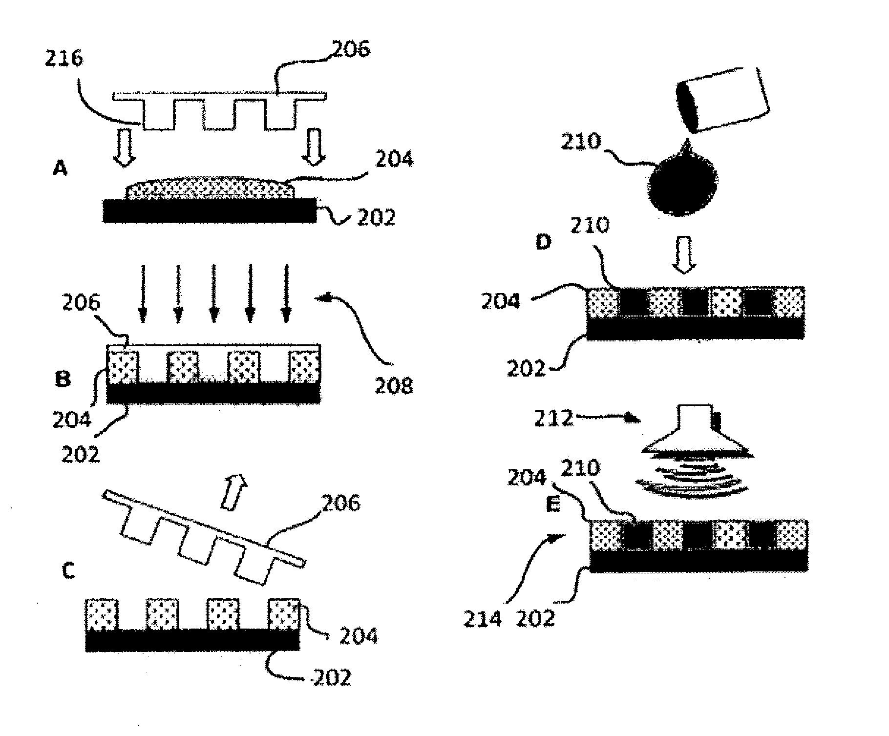
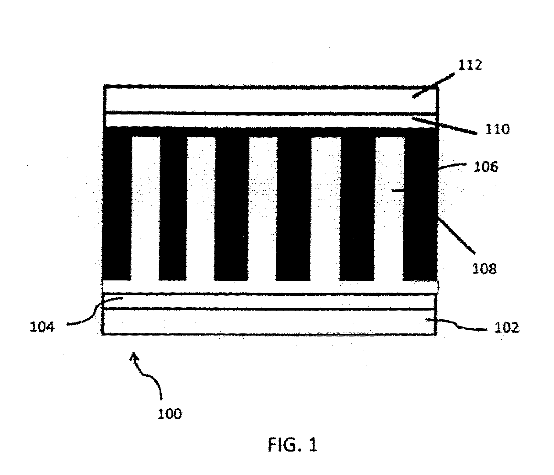
  • High fidelity nano-structures and arrays for photovoltaics and methods of making the same
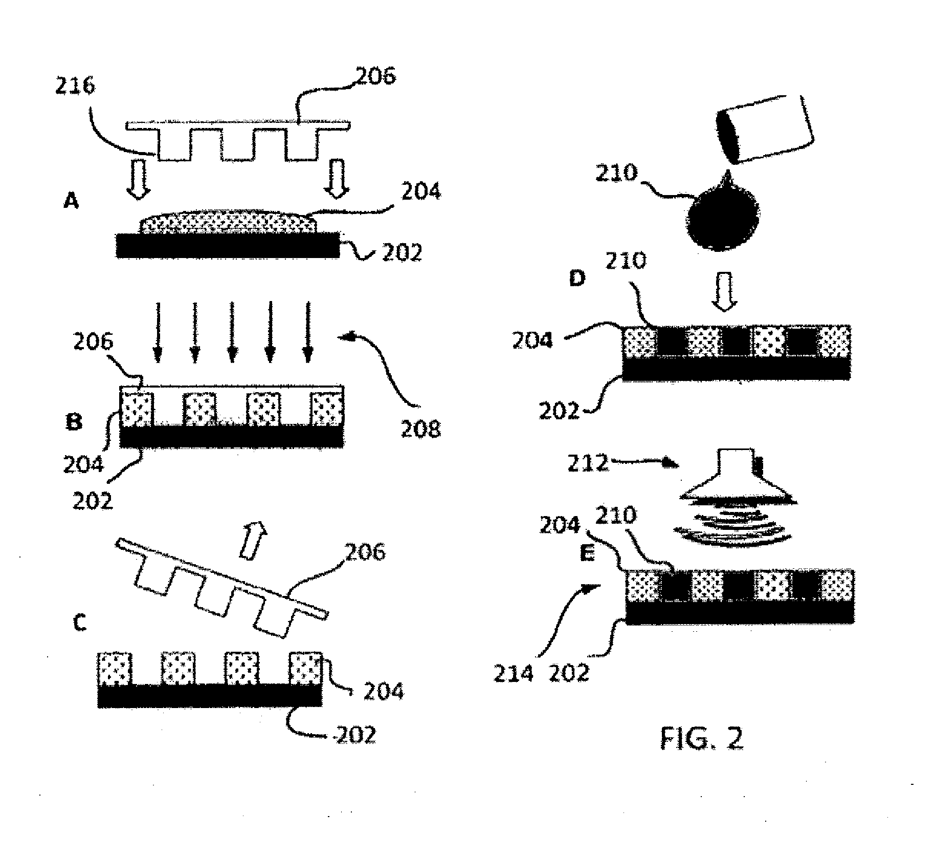
  • High fidelity nano-structures and arrays for photovoltaics and methods of making the same
  • High fidelity nano-structures and arrays for photovoltaics and methods of making the same

Examples


example 1

Fabrication of a Generic Polymer-Polymer BHJ PV Cell

[0093]A patterned perfluoropolyether (PFPE) mold can be generated by pouring a PFPE-dimethacrylate (PFPE-DMA) containing 1-hydroxycyclohexyl phenyl ketone over a silicon substrate patterned with 140 nm lines separated by 70 nm. A poly(dimethylsiloxane) mold can be used to confine the liquid PFPE-DMA to the desired area.

[0094]The apparatus can then be subjected to UV light (λ=365 nm) for 10 minutes while under a nitrogen purge. Next, the fully cured PFPE-DMA mold is released from the silicon master. Separately, an ITO glass substrate will be pre-treated with acetone and isopropanol in an ultrasonic bath followed by cleaning for 10 minutes with oxygen plasma. The ITO substrate will be then treated with a non-wetting silane agent and an adhesion promoter. Following this, the electron donor material will be blended with a photoinitiator, a sample placed on the treated ITO substrate, and the patterned PFPE mold placed on top of it. The ...

example 2

Fabrication of PV Cell Using OVPD to Obtain Nanostructured BHJ's

[0096]A patterned perfluoropolyether (PFPE) mold can be generated by pouring a PFPE-dimethacrylate (PFPE-DMA) containing 1-hydroxycyclohexyl phenyl ketone over a silicon substrate patterned with 140 nm lines separated by 70 nm. A poly(dimethylsiloxane) mold can be used to confine the liquid PFPE-DMA to the desired area.

[0097]The apparatus will then be subjected to UV light (λ=365 nm) for 10 minutes while under a nitrogen purge. Next, the fully cured PFPE-DMA mold is released from the silicon master. Separately, an ITO glass substrate will be pre-treated with acetone and isopropanol in an ultrasonic bath followed by cleaning for 10 minutes with oxygen plasma. Using organic vapor-phase deposition (OVPD), copper phthalocyanine (CuPc) can be deposited onto the PFPE mold so that the features are filled and a uniform layer of CuPc connects each feature. The ITO substrate can then be treated with an adhesion promoter and the e...

example 4

Fabrication of Isolated “Flash Free” Features for Microelectronics

[0100]A patterned perfluoropolyether (PFPE) mold is generated by pouring a PFPE-dimethacrylate (PFPE-DMA) containing 1-hydroxycyclohexyl phenyl ketone over a silicon substrate patterned with 140 nm lines separated by 70 nm. A poly(dimethylsiloxane) mold is used to confine the liquid PFPE-DMA to=365 nm) for the desired area. The apparatus is then subjected to UV light (λ 10 minutes while under a nitrogen purge. The fully cured PFPE-DMA mold is then released from the silicon master. Separately, TMPTA is blended with 1 wt % of a photoinitiator, 1-hydroxycyclohexyl phenyl ketone. Flat, uniform, non-wetting surfaces capable of adhering to the resist material are generated by treating a silicon wafer cleaned with “piranha” solution (1:1 concentrated sulfuric acid: 30% hydrogen peroxide (aq) solution) and treating the wafer with a mixture of an adhesion promoter, (trimethoxysilyl propyl methacryalte) and a non-wetting silane...


PUM

PropertyMeasurementUnit
distanceaaaaaaaaaa
distanceaaaaaaaaaa
distanceaaaaaaaaaa

Abstract

A photovoltaic device includes an electron accepting material and an electron donating material. One of the electron accepting or donating materials is configured and dimensioned as a first component of a bulk heterojunction with a predetermined array of first structures, each first structure is substantially equivalent in three dimensional shape, has a substantially equivalent cross-sectional dimension, and where each first structure of the array of first structures has a substantially equivalent orientation with respect to adjacent first structures of the predetermined array forming a substantially uniform array.

Description

CROSS REFERENCE TO RELATED APPLICATIONS[0001]This application is based on and claims priority to U.S. Provisional Patent Application Ser. No. 60 / 798,858, filed May 9, 2006; U.S. Provisional Patent Application Ser. No. 60 / 799,876, filed May 12, 2006; and U.S. Provisional Patent Application Ser. No. 60 / 833,736, filed Jul. 27, 2006, and U.S. Provisional Patent Application Ser. No. 60 / 903,719, filed Feb. 27, 2007; each of which is incorporated herein by reference in its entirety.[0002]This application is also a continuation-in-part of U.S. patent application Ser. No. 10 / 583,570, filed Jun. 19, 2006, which is the national phase entry of PCT International Patent Application Serial No. PCT / US04 / 42706, filed Dec. 20, 2004, which is based on and claims priority to U.S. Provisional Patent Application Ser. No. 60 / 531,531, filed on Dec. 19, 2003, U.S. Provisional Patent Application Ser. No. 60 / 583,170, filed Jun. 25, 2004, and U.S. Provisional Patent Application Ser. No. 60 / 604,970, filed Aug. ...

Claims


Application Information

Patent Timeline
Patent Type & Authority Applications(United States)
IPC IPC(8): H01L31/18H01L31/0352
CPCB82Y10/00B82Y20/00B82Y30/00B82Y40/00G03F7/0002H01L31/0352H01L31/18H01L51/0036H01L51/0047H01L51/422H01L51/4253Y02E10/549H01L51/0004B81C1/00031B81C2201/034B29C39/36H10K71/13H10K85/113H10K85/215H10K30/15H10K30/35H10K30/50B29C37/0003B81C1/00214B81C99/0085H10K30/30
Inventor DESIMONE, JOSEPH M.ROTHROCK, GINGER DENISONZHOU, ZHILIANSAMULSKI, EDWARD T.EARL, MEREDITHWILLIAMS, STUART
Owner THE UNIV OF NORTH CAROLINA AT CHAPEL HILL
Learn More