Plasma Etch Resistant, Highly Oriented Yttria Films, Coated Substrates and Related Methods

a technology of yttria film and substrate, applied in the direction of molten spray coating, vacuum evaporation coating, coating, etc., can solve the problems of increasing production cost, reducing the resistance of substrates to etching, so as to increase the plasma resistance of substrates and increase the resistance to degradation

Inactive Publication Date: 2013-10-24
GREENE TWEED TECH
View PDF0 Cites 12 Cited by
  • Summary
  • Abstract
  • Description
  • Claims
  • Application Information

AI Technical Summary

Benefits of technology

[0010]Methods of increasing the plasma resistance of substrate are also included. These methods include depositing a yttria material-containing composition onto at least a portion of a surface of a substrate to form a film. The film comprises a yttria material and at least a portion of the yttria material is in a crystal phase having an orientation defined by a Miller Index notation {111}. The portion of the substrate bearing the film exhibits an increased resistance to degradation upon exposure to plasma.

Problems solved by technology

These materials, however, may be easily eroded during routine processing conditions whether chemically, physically, and / or thermally.
Although these films often exhibit improved plasma resistance in the form of reduced weight loss, they still frequently generate unwanted particulates.
Particulates liberated in the processing chamber result in damaged or flawed wafers, which must then be discarded, greatly increasing the cost of production and reducing production line efficiency.
Subsequently, the aluminum fluoride particulates shed off the chamber walls and contaminate the wafers.
Thermal-sprayed yttria films, however, are porous and generate unwanted particulates.

Method used


Image

  • Plasma Etch Resistant, Highly Oriented Yttria Films, Coated Substrates and Related Methods
  • Plasma Etch Resistant, Highly Oriented Yttria Films, Coated Substrates and Related Methods
  • Plasma Etch Resistant, Highly Oriented Yttria Films, Coated Substrates and Related Methods

Examples


example i

[0046]Two sets of yttrium oxide films were grown on fused quartz coupons (dimensions: 1 inch×1 inch; ⅛ inch thick) by electron beam evaporation. Each coupon was installed in the electron beam film chamber and the chamber was vacuum purged overnight. The film chamber vacuum level was maintained at 2.4×10⁻⁵ ton and preheated for 12 hours to ensure temperature equilibrium was reached.

[0047]High purity (>99.99%) Y2O3 target was evaporated by electron beam and each coupon was coated for 4 hours to reach target thickness of about 4 microns. During the film process, temperature of the substrate was maintained between about 150° C. to about 350° C.

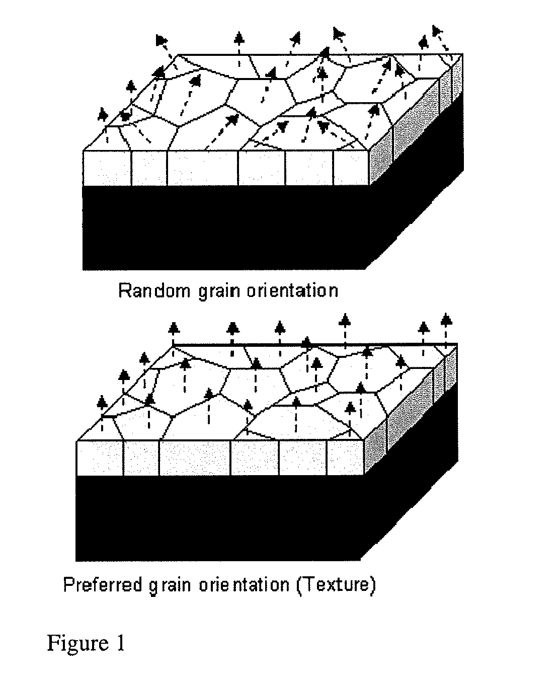
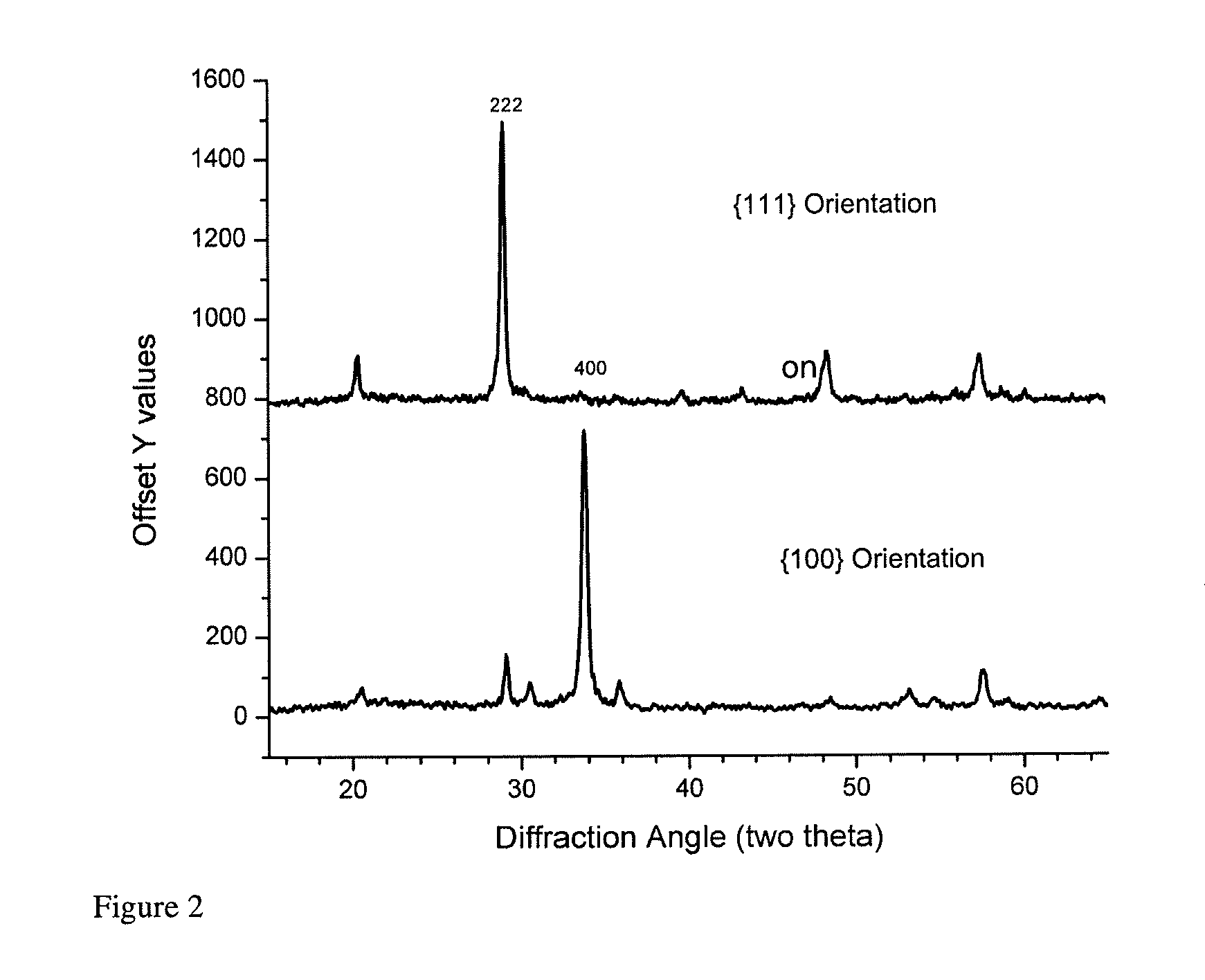
[0048]One set of films was grown to predominantly produce a crystalline structure having an orientation described by Miller Index notation {100}. The second set was grown to produce predominantly a crystalline structure having an orientation described by Miller Index notation {111}.

[0049]FIG. 2 shows x-ray diffraction (XRD) measurements of the two...


PUM

PropertyMeasurementUnit
thicknessaaaaaaaaaa
thicknessaaaaaaaaaa
thicknessaaaaaaaaaa

Abstract

Included within the scope of the invention are plasma etch-resistant films for substrates. The films include a yttria material and a at least a portion of the yttria material is in a crystal phase having an orientation defined by a Miller Index notation {111}. Also included are methods of manufacturing plasma etch-resistant films on a substrate. Such methods include applying a yttria material-containing composition onto at least a portion of a surface of a substrate to form a film. The film includes a yttria material and at least a portion of the yttria material is in a crystal phase having an orientation defined by a Miller Index notation {111}.

Description

CROSS REFERENCE TO RELATED APPLICATION[0001]This application claims the benefit under 35 U.S.C. §119(e) of U.S. Provisional Patent Application No. 61 / 406,445, filed Oct. 25, 2010, the entire disclosure of which is incorporated herein by reference.BACKGROUND OF THE INVENTION[0002]Resistance to plasmas is a desirable property for components used in processing chambers where corrosive environments are present. Process chambers and component apparatus present within or used in conjunction with processing chambers which are used in the fabrication of electronic devices and MEMS are frequently constructed from various substrates such as sapphire, silica, fused silica, quartz, fused quartz, alumina, sapphire, silicon, aluminum, anodized aluminum, zirconium oxide, and an aluminum alloy, as these materials are known to have a level of plasma resistance.[0003]These materials, however, may be easily eroded during routine processing conditions whether chemically, physically, and / or thermally. T...

Claims


Application Information

Patent Timeline
Patent Type & Authority Applications(United States)
IPC IPC(8): C23F11/00
CPCC23F11/00C23C14/083C23C16/4404C23C4/11C23C4/134
Inventor AHEEM, MOHAMMED MAHBUBULALEXANDER, WILLIAM BROCKLEE, SANG-HOMERCER, THOMASVORSA, VASIL
Owner GREENE TWEED TECH
Why Eureka
Try Eureka