Graphene-based semiconductor device

a graphene-based, semiconductor technology, applied in the direction of semiconductor devices, electrical appliances, nanotechnology, etc., can solve the problems of limiting factors affecting the use of graphene in logic applications, unable to switch off, and poor ion/ioff of transistors using slg as active channels,

Active Publication Date: 2013-11-28
INTERUNIVERSITAIR MICRO ELECTRONICS CENT (IMEC VZW) +1
View PDF17 Cites 37 Cited by
  • Summary
  • Abstract
  • Description
  • Claims
  • Application Information

AI Technical Summary

Benefits of technology

[0061]In an embodiment of the second aspect, the present disclosure relates to a method for manufacturing a field effect transistor, comprising the steps of: providing a substrate comprising an electrically conductive part (herein named “second electrode”) and an electrically insulating part (herein named “second” insulating layer), providing a dopant layer on said electrically insulating part, said dopant layer being suitable for creating said free charge carriers of a second type, opposite to a first type, in a second graphene layer, depositing a bilayer graphene, comprising a first and said second graph

Problems solved by technology

As a consequence, transistors using SLG as active channel exhibit a poor Ion/Ioff (generally ˜10), and cannot be switched off.
This is one of the main limiting factors hampering the use of graphene in microelectronics for logic applications.
However, the doping approaches listed above are not easily controlled as the dopants tend to

Method used


Image

  • Graphene-based semiconductor device
  • Graphene-based semiconductor device
  • Graphene-based semiconductor device

Examples


example 1

Preparation of a Field-Effect Transistor Using an Electrically Insulating Layer Comprising Polystyrene and a p-Dopant

Substrate Preparation:

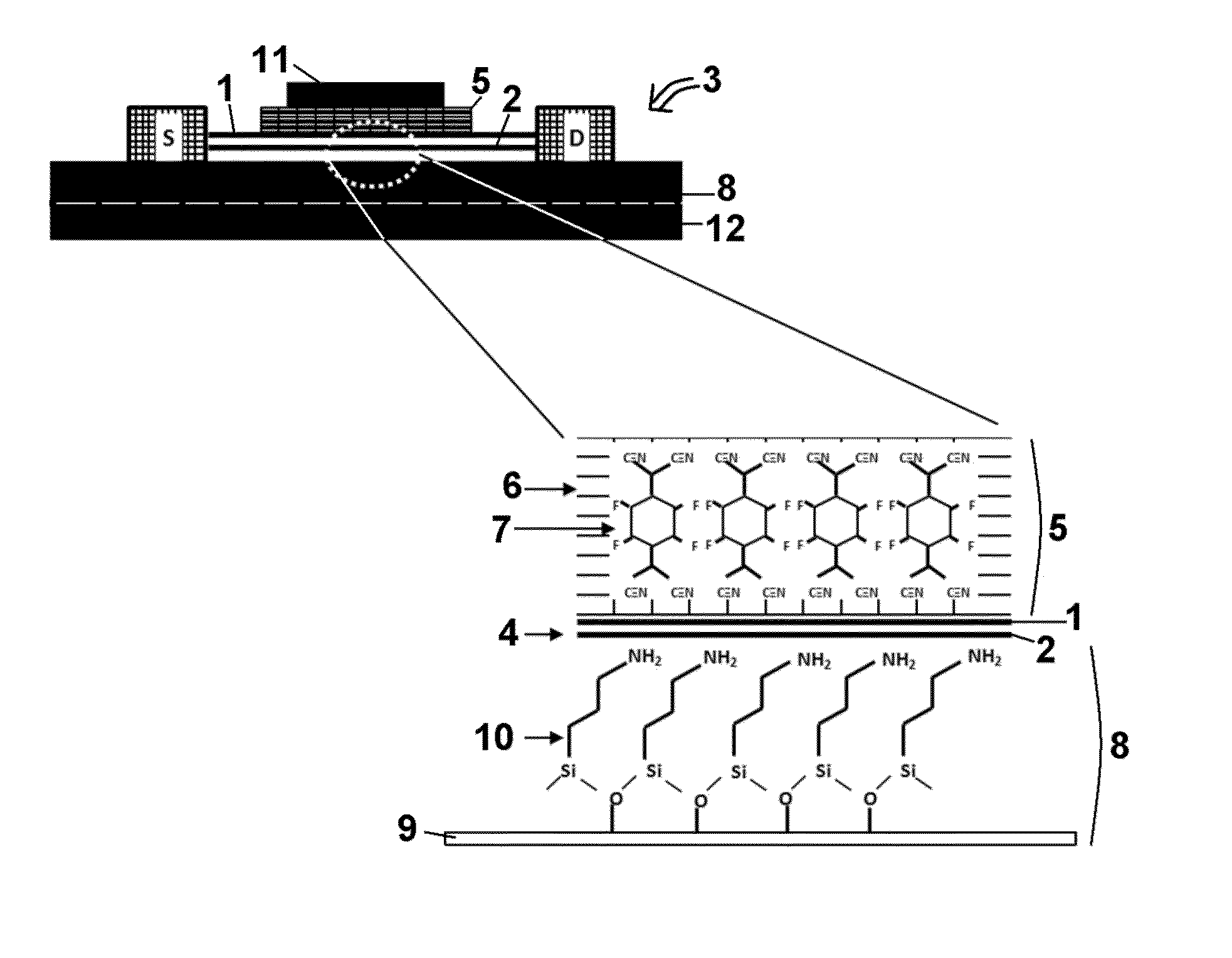
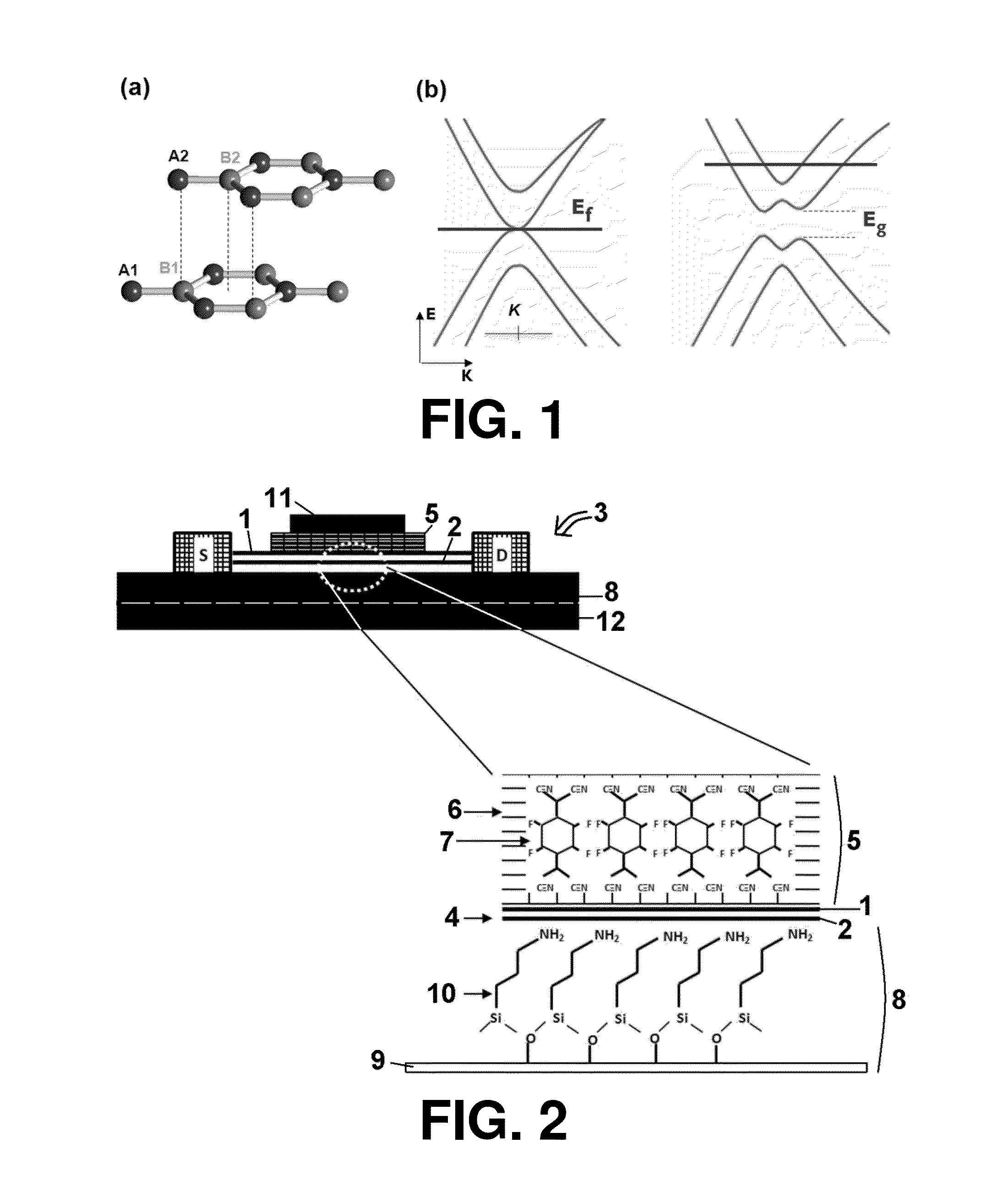
[0075]Substrates consisting of Si wafers (12, see FIG. 2) with 300 nm thermally grown Si oxide were cleaned for 10 min in a 1:1:5 NH4OH:H2O2:H2O solution (75° C.) to remove contaminants.

[0076]Substrate silanization was then carried out by vertically dipping the substrate in a 0.5% vol. 3-aminopropyl triethoxysilane solution (APTES) in anhydrous toluene for 1 h, rinsing well with toluene and sonicating in isopropanol to remove noncovalently bonded silane molecules. A self assembled monolayer (SAM, 10 see FIG. 2) was thereby obtained.

[0077]The sample was then further annealed under N2 atmosphere at 120° C. to improve the quality of SAM.

Graphene Deposition:

[0078]Samples bearing a single layer graphene and samples bearing a bilayer graphene were prepared. For this purpose, SLG and BLG were respectively deposited on silanized substrates by micromechan...

example 2

Coupling of a Top Gate Electrode to the Electrically Insulating Layer Comprising Polystyrene and a p-Dopant

[0109]A top gate electrode is defined on the electrically insulating layer by optical lithography.

[0110]This has the advantage over Example 1 to permit an increase of the magnitude of the induced electrical field. Thereby, the device benefits from both external and molecular gates.

example 3

Preparation of a Field-Effect Transistor (3) Using an Electrically Insulating Layer (5) Comprising a High-k Polymer (6) and a p-Dopant (7), Said Insulating Layer (5) being Coupled to a Top Gate Electrode (11)

[0111]Referring to FIG. 2, for the preparation of a field-effect transistor (3) using an electrically insulating layer (5), the same procedure as described in Example 1 is repeated except that in the preparation of the polymer (6) / F4TCNQ (7) blends (5), a high-k polymer (6) (having a relative permittivity of at least 4.0) is used instead of polystyrene. Typically, Poly(trifluoroethylene) or poly(vinylidene fluoride) is used.

[0112]Similarly to Example 1, high-k polymer (6) / F4TCNQ (7) blends (5) with different concentrations are prepared and the dielectric constant and break-down voltage of each blend (5) is measured in order to find the optimum concentration of F4TCNQ (7).

[0113]For the Coupling of a top gate electrode (11) to the high-k electrically insulating layer (5), the same...


PUM


Abstract

A semiconductor device is provided comprising a bilayer graphene comprising a first and a second adjacent graphene layer, and a first electrically insulating layer contacting the first graphene layer, the first electrically insulating layer comprising an electrically insulating material, and a substance suitable for creating free charge carriers of a first type in the first graphene layer, the semiconductor device further comprising an electrically insulating region contacting the second graphene layer and suitable for creating free charge carriers of a second type, opposite to the first type, in the second graphene layer.

Description

INCORPORATION BY REFERENCE TO RELATED APPLICATIONS[0001]Any and all priority claims identified in the Application Data Sheet, or any correction thereto, are hereby incorporated by reference under 37 CFR 1.57. This application claims the benefit of European Application No. EP 12168995.4 filed on May 23, 2012, the disclosure of which is hereby expressly incorporated by reference in its entirety and is hereby expressly made a portion of this application.TECHNICAL FIELD[0002]The present disclosure relates to semiconductor devices comprising a bilayer graphene as well as to method for the manufacturing thereof. In particular, the present disclosure relates to field effect transistors.BACKGROUND[0003]Graphene is a 2-dimensional, semi-metallic, atomically-thin film in which carbon atoms are arranged into a sp2 honeycomb lattice structurally relying on in-plane, covalent σ-bonds. It has been successfully isolated for the first time in 2004 at the University of Manchester by A. K. Geim, K. S...

Claims


Application Information

Patent Timeline
IPC IPC(8): H01L29/16H01L21/02
CPCH01L29/1606H01L21/02376Y10S977/734B82Y40/00H01L29/778H01L29/4908H01L29/78603H01L29/78684H01L29/78696H01L21/02527H01L21/02612H10K10/486H01L29/772
Inventor NOURBAKHSH, AMIRHASANCANTORO, MIRCOHUYGHEBAERT, CEDRICHEYNS, MARCDE GENDT, STEFAN
Owner INTERUNIVERSITAIR MICRO ELECTRONICS CENT (IMEC VZW)
Why Eureka
Try Eureka