
Method For The Detection Of Defects In Gas-Barrier Films Using Quantum Dots

a gasbarrier and quantum dots technology, applied in the field of thin film gasbarriers, can solve the problems of affecting the stability and performance of electronic devices, affecting the performance of optical radiation measurement, and affecting the stability of electronic devices

Active Publication Date: 2013-11-28
SAMSUNG ELECTRONICS CO LTD
View PDF5 Cites 7 Cited by
  • Summary
  • Abstract
  • Description
  • Claims
  • Application Information

AI Technical Summary

Benefits of technology

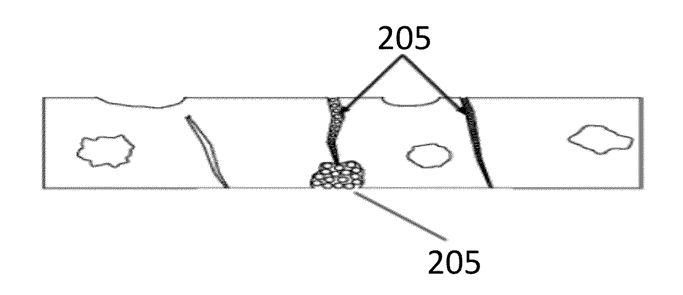
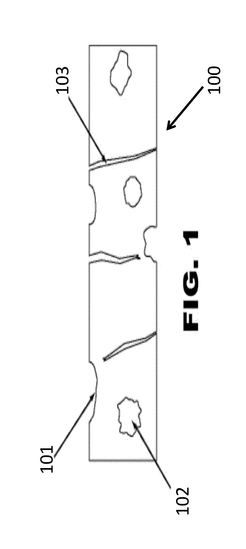
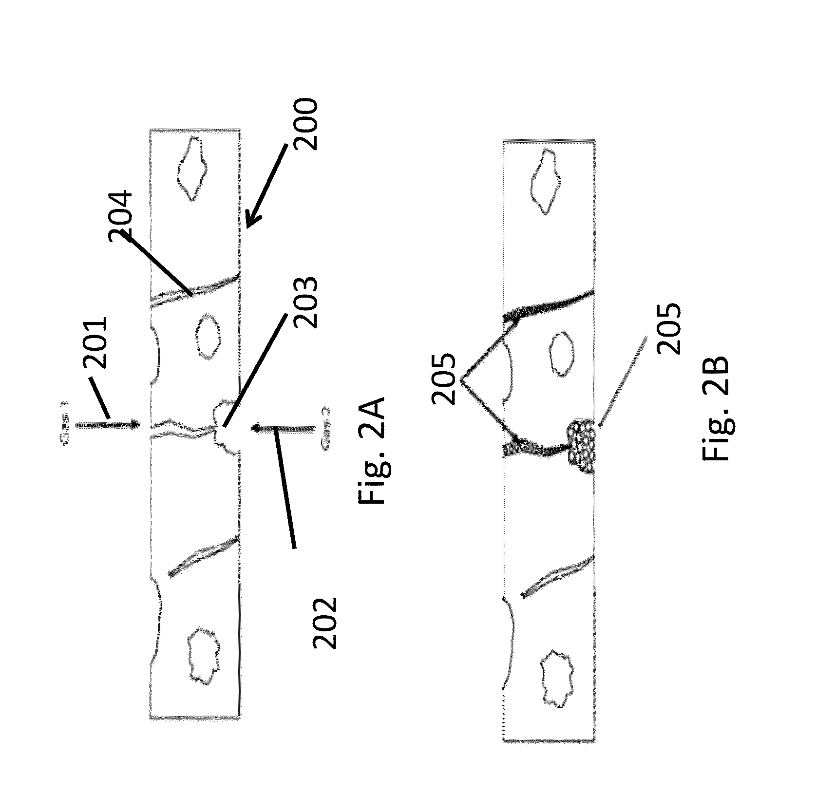
The present patent describes a method for synthesizing quantum dots (QDs) using gas precursors within defects in gas-barrier films. This allows for the detection of defects in the film, such as channel cracks and open pores, by visualizing the emission from the QDs. The optical properties of the QDs can be used to determine the particle size and nature of the defects. The technical effects of this method include improved accuracy in defect detection and characterization, as well as improved efficiency in the production of QDs.

Problems solved by technology

Gases such as O2 and water vapor can detrimentally affect the stability and performance of electronic devices.
However, such pores are still undesirable as they may weaken the film.
Full-thickness cracks compromise the film integrity by allowing gas molecules to diffuse through, potentially reducing the device stability and performance.
Defects in contact with just one surface of a film are also undesirable since they have the potential to propagate to full-thickness cracks.
However, the 3 nm lower detection limit of mercury intrusion porosimetry is inadequate for verification of the integrity of gas-barrier films, since molecules of water and oxygen are an order of magnitude smaller and may diffuse through much narrower cracks.
Further, mercury intrusion porosimetry may be used to give an indication of defect diameter, but does not provide any visual representation of the defect structure.
The model assumes a cylindrical pore shape, which is not always accurate.
Using conventional apparatus, the detection area is also limited to approximately 1 cm2, so larger films cannot be characterized by this technique.
The technique relies upon high operating pressures, which may be damaging to the film or electronic device.
These high pressures may be particularly detrimental when a sample contains many closed pores, which cannot be detected using this technique, as the high pressures may compress a sample.
Therefore, it may be inaccurate in characterizing the pore distribution in systems wherein the pore structure deviates from these criteria.
In addition, the acquisition of a single measurement may take several hours.
Other drawbacks include the fact that the sample may come into contact with liquid nitrogen during the course of the measurement, which may result in damage to the sample, and cryogenic temperatures are required to ensure little attraction between the gas-phase molecules, which may be difficult and costly to maintain.

Method used


Image

  • Method For The Detection Of Defects In Gas-Barrier Films Using Quantum Dots
  • Method For The Detection Of Defects In Gas-Barrier Films Using Quantum Dots
  • Method For The Detection Of Defects In Gas-Barrier Films Using Quantum Dots

Examples


example 1

CdS

[0042]CdS quantum dots may be formed from the gas phase reaction of helium gas streams containing Me2Cd and H2S in the presence of pyridine gas. Typical reaction conditions include a He flow rate of ˜600 cm3 min−1 and a 30-fold excess of H2S to Me2Cd. The particle size may be controlled by varying the pyridine concentration and / or the reaction temperature. Preferably, pyridine:Me2Cd ratios in the range 1:20 to 2:1, and temperatures between room temperature and 200° C. are employed. It has been found that increasing the pyridine concentration reduces the particle size, while the particle size increases with increasing temperature.

[0043]The absorption of the CdS nanoparticles may be tuned from the UV to cyan (bulk band gap ˜512 nm) depending on the particle size. For example, nanoparticles in the size range 2-20 nm may be expected to emit between approximately 320-500 nm, corresponding with UV to cyan light.

example 2

CdSe

[0044]Reaction conditions similar to those outlined for CdS (above) may be used to synthesize CdSe quantum dots [N. L. Pickett et al., J. Mater. Chem., 1997, 7, 1855], substituting H2S for H2Se. Higher pyridine concentrations may be used to control the particle size (up to 150:1 pyridine:Me2Cd).

[0045]The absorption of the CdSe nanoparticles may be tuned from the blue to the deep red (bulk band gap ˜717 nm) depending on the particle size. Nanoparticles in the size range 2-20 nm may be expected to emit between approximately 490-700 nm, corresponding with blue to deep red light.

example 3

ZnS

[0046]Reaction conditions similar to those outlined for CdS (above) may be used to synthesize ZnS quantum dots [N. L. Pickett et al., J. Mater. Chem., 1997, 7, 1855], substituting Me2Cd for Me2Zn. Higher reaction temperatures (up to 300° C.) may be advantageous.

[0047]The absorption of the ZnS nanoparticles may be tuned across the UV spectrum (bulk band gap ˜344 nm) depending on the particle size. Nanoparticles in the size range 2-20 nm may be expected to emit between approximately 235-340 nm.


PUM

PropertyMeasurementUnit
pore diametersaaaaaaaaaa
diametersaaaaaaaaaa

Abstract

By forming nanoparticles from gas-phase precursors within cracks or defects in a gas-barrier film, crack-width may be determined from the diameter of the nanoparticles formed within. The optical absorption and emission wavelengths of a quantum dot are governed by the particle size. For a particular material, the absorption and / or emission wavelengths may therefore be correlated to the particle size (as determined from techniques such as transmission electron microscopy, TEM). Thus, fluorescence measurement techniques and / or confocal microscopy may be used to determine the size of quantum dots formed within a gas-barrier film, allowing both the size and nature of a defect to be determined. The method may be used to assess the potential effects of defects on the integrity of the gas-barrier film.

Description

RELATED APPLICATIONS[0001]This application claims the benefit of U.S. Provisional Application No. 61 / 642,934, filed May 4, 2012, the entire contents of which are hereby incorporated herein by reference.BACKGROUND[0002]This invention relates to thin film gas-barriers. More particularly, it relates to methods for characterizing thin film gas-barriers using gas-phase synthesis of quantum dots.[0003]In the electronics industry, much work has been carried out into the development of effective gas-barriers for electronic devices. Gases such as O2 and water vapor can detrimentally affect the stability and performance of electronic devices. Therefore a gas-barrier film may be applied on top of the active device layer to shield the active layer from such contaminants. In addition, gas-barrier films may impart functionality, such as flexibility or shock-resistance, to electronic devices.[0004]Gas-barrier films are employed in other areas in addition to the electronics industry. For example, i...

Claims


Application Information

Patent Timeline
Patent Type & Authority Applications(United States)
IPC IPC(8): G01N21/64G01N21/59
CPCG01N21/64G01N21/59G01N21/91G01N21/6489G01N2021/8427G01N2015/0813
Inventor PICKETT, NIGELGRESTY, NATHALIE
Owner SAMSUNG ELECTRONICS CO LTD
Learn More