Thin film condenser for high-density packaging, method for manufacturing the same, and high-density package substrate including the same

a technology of high-density packaging and thin film, which is applied in the direction of fixed capacitor details, electrical apparatus casings/cabinets/drawers, instruments, etc., can solve the problems of high cost and low yield, degradation of product quality, and large connection length between devices at high frequency, and achieves excellent capacitance and dielectric properties, simple structure, and easy embedding in high-density package substrates

Inactive Publication Date: 2013-11-28
KOREA INST OF SCI & TECH
View PDF7 Cites 5 Cited by
  • Summary
  • Abstract
  • Description
  • Claims
  • Application Information

AI Technical Summary

Benefits of technology

[0037]The thin film condenser for high-density packaging disclosed herein has a simple structure and is capable of being embedded in a high-density package substrate easily without changing the electrical and physical properties of the high-density package substrate. In addition, the thin film condenser for high-density packaging has excellent capacitance and dielectric properties.
[0038]Additionally, since the thin film condenser disclosed herein does not have a complicated structure that appears in the case of the thin film condenser for high-density packaging according to the related art but has a simple structure, it is manufactured with ease at low cost. Further, the high-density package substrate disclosed herein has thin film condensers packaged with high density, and thus has high packaging efficiency per unit area (or volume) and realizes a slimmed appearance.

Problems solved by technology

By virtue of highly integrated packaging of a circuit and a decrease in connection length, the condensers for high-density packaging obtained by the above methods may overcome degradation of reliability of finished products caused by an increase in connection number through soldering or the like and by degradation of product quality resulting from a large connection length between devices at high frequency in the existing surface mounting devices and generation of electrically parasitic components.
Therefore, they have problems of high cost and low yield, since the internal structures for device connection are complicated and the condensers are realized only by repeating a complicated process such as photolithography many times. Moreover, since the condensers have a plurality of layers, it is difficult to package (embed) them in a high-density package substrate.
This results in a change in electrical and physical properties of a high-density package substrate, and degradation of capacitance and dielectric properties.

Method used


Image

  • Thin film condenser for high-density packaging, method for manufacturing the same, and high-density package substrate including the same
  • Thin film condenser for high-density packaging, method for manufacturing the same, and high-density package substrate including the same
  • Thin film condenser for high-density packaging, method for manufacturing the same, and high-density package substrate including the same

Examples


example 1

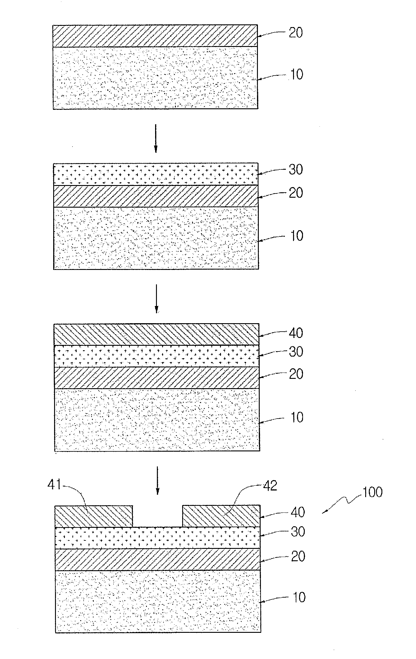
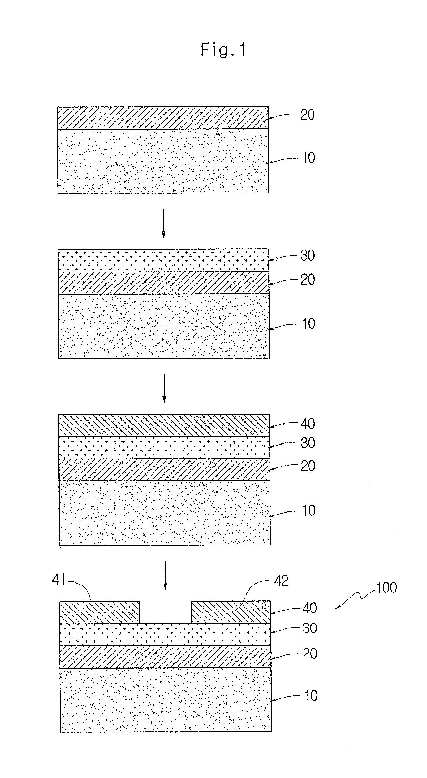
[0099]To form a dielectric thin film on the support substrate on which the Pt lower electrode is deposited as described above, an RF-sputtering process is used. The 2-inch BaTiO3 target obtained from Preparation Example 1 is used as a material for the dielectric thin film. To prevent the thin film from being contaminated during deposition, a high vacuum state of about 2×10⁻⁶ torr is maintained before deposition. In addition, Ar and O2 gases are maintained at a ratio of 9:1 for the purpose of thin film deposition, and then 80 W-RF power is applied under a vacuum degree of 20 mtorr. Herein, the heater provided on the bottom of the support substrate is used to maintain a temperature of 700° C. during deposition to assist improvement of the crystallinity of the thin film.

[0100]Deposition is carried out for 50 minutes under the above-mentioned conditions to form a BaTiO3 thin film with a thickness of about 100 nm. After the deposition, a rapid thermal annealing system is used to perform ...

example 2

[0103]To form a dielectric thin film on the support substrate on which the Pt lower electrode is deposited as described above, an RF-sputtering process is used. The 2-inch Ba0.6Sr0.4TiO3 target obtained from Preparation Example 2 is used as a material for the dielectric thin film. To prevent the thin film from being contaminated during deposition, a high vacuum state of about 2×10⁻⁶ torr is maintained before deposition. In addition, Ar and O2 gases are maintained at a ratio of 8:2 for the purpose of thin film deposition, and then 80 W—RF power is applied under a vacuum degree of 20 mtorr. Herein, the heater provided on the bottom of the support substrate is used to maintain a temperature of 700° C. during deposition to assist improvement of the crystallinity of the thin film.

[0104]Deposition is carried out for 65 minutes under the above-mentioned conditions to form a Ba0.6Sr0.4TiO3 thin film with a thickness of about 100 nm. After the deposition, a rapid thermal annealing system is ...

example 3

[0107]To form a dielectric thin film on the support substrate on which the Pt lower electrode is deposited as described above, a sol-gel process is used. The Ba0.6Sr0.4TiO3 solution for a sol-gel process obtained from the above Preparation Example is used as a material for the dielectric thin film. First, the Ba0.6Sr0.4TiO3 solution is dropped onto the support substrate and spin-coated at 500 rpm for 5 seconds and at 4000 rpm for 30 seconds, followed by drying at 150° C. for 5 minutes to remove the solvents. Then, to remove the remaining organic materials, heat treatment is carried out at 350° C. for 10 minutes to form an amorphous Ba0.6Sr0.4TiO3 thin film. It is required that the amorphous Ba0.6Sr0.4TiO3 thin film is converted into a multicrystalline thin film to increase the dielectric constant of the thin film. For this, a rapid thermal annealing system is used to perform heat treatment at 800° C. for 5 minutes.

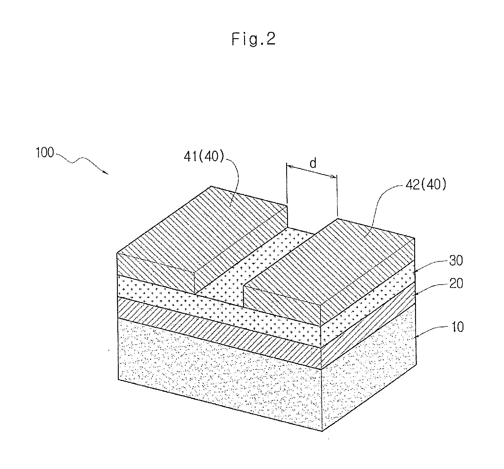
[0108]Then, a DC sputtering process is used to form an upper electrod...


PUM

PropertyMeasurementUnit
thicknessaaaaaaaaaa
thicknessaaaaaaaaaa
relative dielectric constantaaaaaaaaaa

Abstract

Provided are a thin film condenser for high-density packaging, a method for manufacturing the same and a high-density package substrate. The thin film condenser for high-density packaging, includes: a support substrate; a lower electrode formed on the support substrate; a dielectric thin film formed on the lower electrode; and an upper electrode formed on the dielectric thin film. Provided also is a method for manufacturing the same. The high-density package substrate, includes: at least two stacked substrates; thin film condensers embedded in the stacked substrates; an internal connection electrode formed in the stacked substrates and connecting the thin film condensers in series or in parallel; a surface electrode formed on the surface of the outermost substrate among the stacked substrates and connected to the internal connection electrode; and an integrated circuit connected to the surface electrode via a bump.

Description

CROSS-REFERENCE TO RELATED APPLICATION[0001]This application claims priority to Korean Patent Application No. 10-2012-0054827, filed on May 23, 2012, and all the benefits accruing therefrom under 35 U.S.C. §119, the contents of which in its entirety are herein incorporated by reference.BACKGROUND[0002]1. Field[0003]The present disclosure relates to a thin film condenser for high-density packaging, a method for manufacturing the same, and a high-density package substrate including the same. More particularly, the present disclosure relates to a thin film condenser capable of being embedded easily in a substrate without modifying the electrical and physical properties of a high-density package substrate and having excellent capacitance and dielectric properties. The present disclosure also relates to a method for manufacturing a thin film condenser for high-density packaging which allows the manufacture of the above-mentioned thin film condenser by a simple process at low cost, and to...

Claims


Application Information

Patent Timeline
Patent Type & Authority Applications(United States)
IPC IPC(8): H01G4/06H05K5/00
CPCH01G4/06H05K5/0091H01G4/005H01G4/085H01G4/33H01L28/60H01G4/12
Inventor KANG, CHONG YUNKANG, MIN GYUYOON, SEOK JINCHOI, JI WONBAEK, SEUNG HYUBKIM, JIN SANG
Owner KOREA INST OF SCI & TECH
Why Eureka
Try Eureka