Preparation of lamellae for tem viewing

a technology of lamellae and lamellae, which is applied in the direction of electrolysis components, vacuum evaporation coatings, coatings, etc., can solve the problems of destroying much of the original sample, time-consuming work, and too small features to be measured

Active Publication Date: 2013-12-05
FEI CO
View PDF4 Cites 55 Cited by
  • Summary
  • Abstract
  • Description
  • Claims
  • Application Information

AI Technical Summary

Benefits of technology

[0023]It is an object of the invention, therefore, to provide a robust process that can repeatedly produce thin lamella for viewing on a transmission electron microscope.

Problems solved by technology

As features continue to get smaller and smaller, however, there comes a point where the features to be measured are too small for the resolution provided by an ordinary SEM.
Because a sample must be very thin for viewing with transmission electron microscopy (whether TEM or STEM), preparation of the sample can be delicate, time-consuming work.
The disadvantage to these techniques is that they are not site-specific and often require that the starting material be sectioned into smaller and smaller pieces, thereby destroying much of the original sample.
The trench 25 milled on the back side of the region of interest is smaller than the front trench 24 The smaller back trench is primarily to save time, but the smaller trench also prevents the finished sample from falling over flat into larger milled trenches which may make it difficult to remove the specimen during the micromanipulation operation.
Unfortunately, preparation of TEM samples using such prior art methods of sample extraction suffer from a number of shortcomings.
Such methods are typically very time-consuming, about 90 minutes / sample, and labor intensive.
Even though the information that can be discovered by TEM analysis can be very valuable, the entire process of creating and measuring TEM samples has historically been so labor intensive and time consuming that it has not been practical to use this type of analysis for manufacturing process control.
Specifically, the ex-situ method discussed above can be time consuming and difficult to locate a lamella site and the extraction probe must be very carefully moved into position to avoid damaging the sample or the probe tip.
Once a lamella has been completely freed, it can move in unpredictable ways; it can fall over in the trench or in some cases it can actually be pushed up and out of the trench by electrostatic forces.
This movement can make it difficult to locate and / or pick up the lamella with the extraction probe.
The electrostatic attraction between the probe and the sample is also somewhat unpredictable.
If the lamella is successfully transferred to the TEM grid, it can be difficult to get the lamella to adhere to the grid support film rather than the probe tip.
As a result, it can be very difficult to control the precise placement or orientation of the lamella when it is transferred to the TEM grid.
The in-situ method described above provides more control but is considerably more time-consuming.
A significant amount of time is taken up by the steps of attaching the microprobe to the sample, attaching the sample to the sample holder, and cutting the microprobe free.
Full or partial automation of the process of sample removal and transport would not only speed up the process, but it would also reduce the level of expertise required of operators and technicians thus lowering personnel costs.
Because of the precision required to produce thin lamella, the process has not adapted itself to automation.
The thinner the lamella, the more difficult it is to automate the extraction process.
Lamella under 100 nm in thickness, particularly lamella under 70 nm in thickness, are difficult to produce either manually or in an automated fashion.
Slight changes in the positioning of the ion beam can ruin the lamella by producing the lamella at a position that excludes the feature of interest or by altering the thickness.
These factors combine to make the formation of lamella an exceedingly difficult process to automate.

Method used


Image

  • Preparation of lamellae for tem viewing
  • Preparation of lamellae for tem viewing
  • Preparation of lamellae for tem viewing

Examples


Embodiment Construction

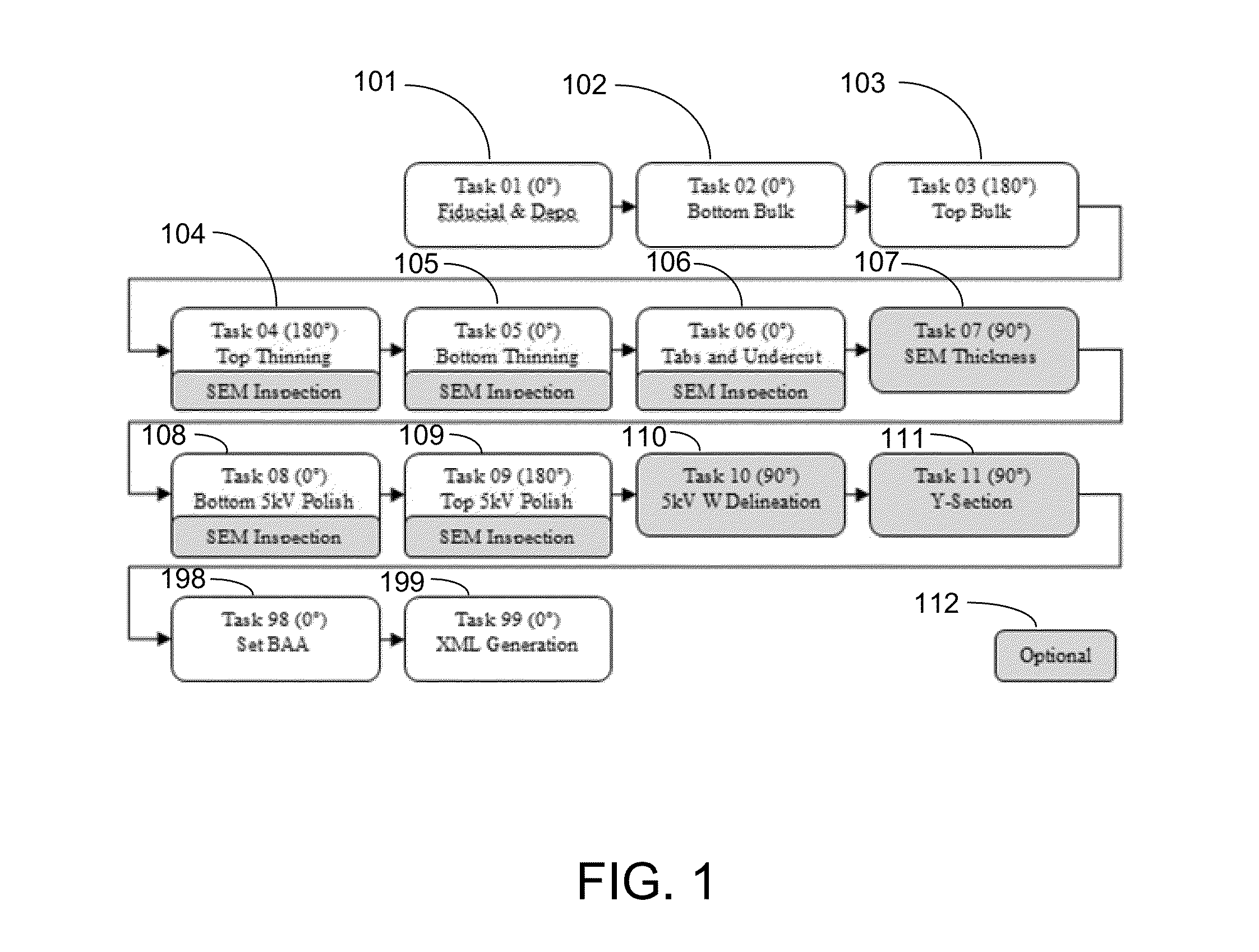
[0053]Preferred embodiments of the present invention are directed toward a method for improved control of lamella placement and sidewall orthogonality. This allows fully automated creation of lamella having a thickness of less than 100 nm, less than 70 nm lamella, or less than 50 nm lamella.

[0054]Embodiment of the invention as described below produce a lamella in which the thickness of the viewing area of the finished lamella preferably varies by less than 25%, more preferably by less than 10%, and even more preferably by less than 3% over the viewing area. The faces of the finished lamella are preferably orthogonal to the substrate surface within 5 degrees, more preferably within 1 degree and even more preferably within 0.5 degrees.

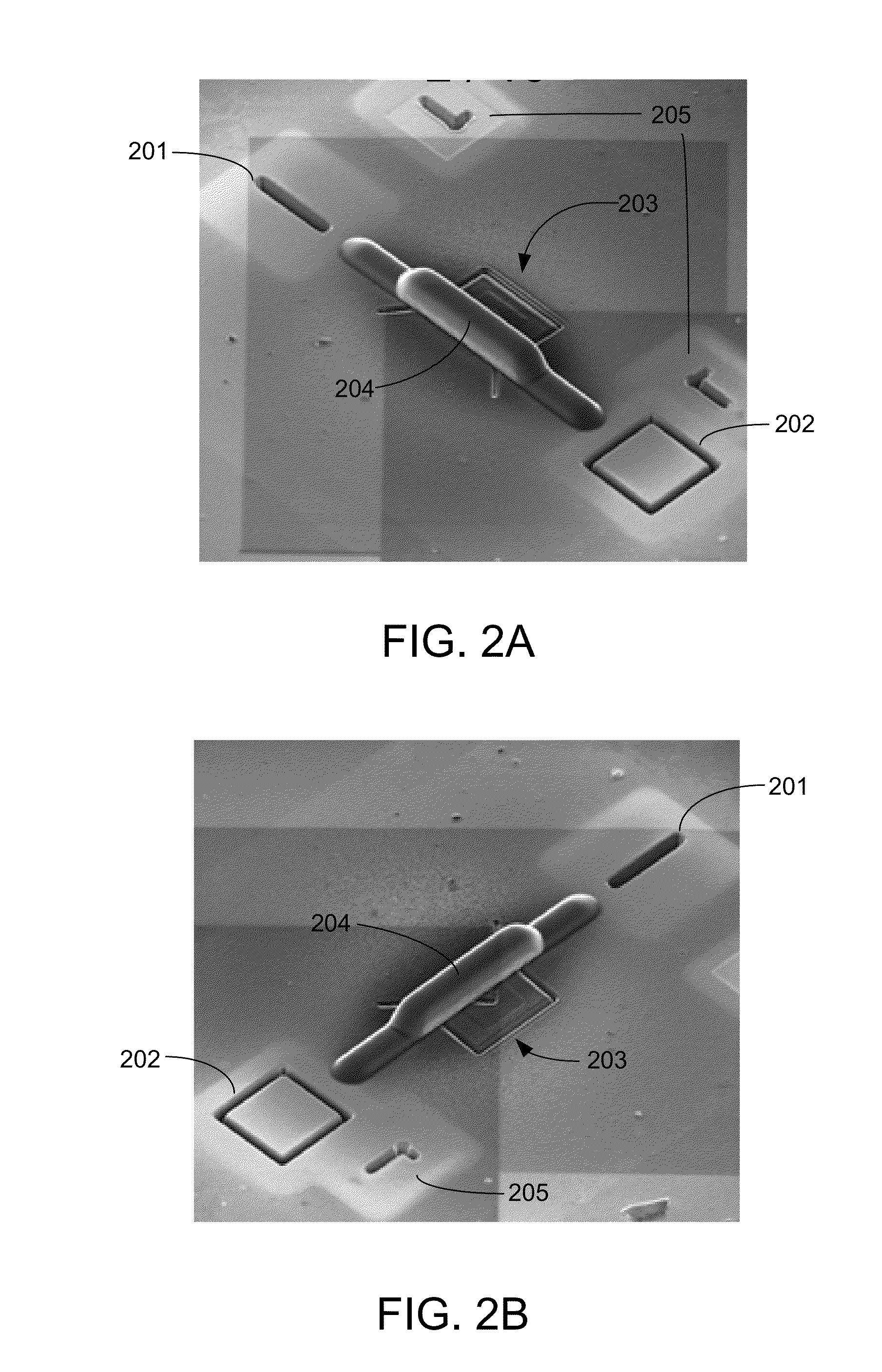
[0055]The viewing area of the finished lamella is typically between 0.2 μm and 5 μm wide and up to 2 μm deep.

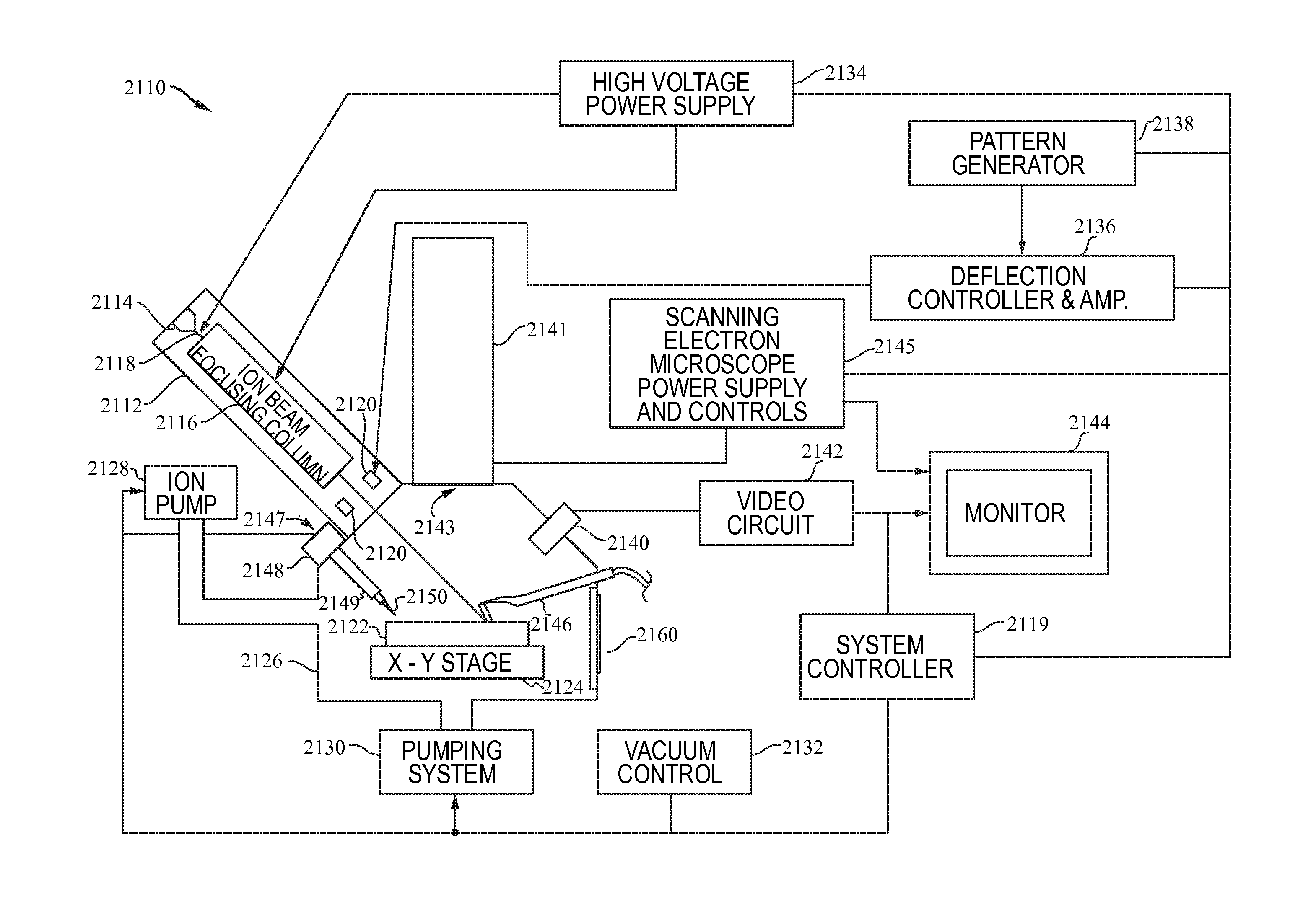
[0056]FIG. 1 shows an overview of a process according to an embodiment of the present invention. The individual steps are described in more detai...


PUM

PropertyMeasurementUnit
landing energyaaaaaaaaaa

Abstract

A method and apparatus for producing thin lamella for TEM observation. The steps of the method are robust and can be used to produce lamella in an automated process. In some embodiments, a protective coating have a sputtering rate matched to the sputtering rate of the work piece is deposited before forming the lamella. In some embodiments, the bottom of the lamella slopes away from the feature of interest, which keeps the lamella stable and reduces movement during thinning. In some embodiments, a fiducial is used to position the beam for the final thinning, instead of using an edge of the lamella. In some embodiments, the tabs are completed after high ion energy final thinning to keep the lamella more stable. In some embodiments, a defocused low ion energy and pattern refresh delay is used for the final cut to reduce deformation of the lamella.

Description

[0001]This Application claims priority from U.S. Provisional Application 61 / 649,917, filed May 21, 2012, which is hereby incorporated by reference.TECHNICAL FIELD OF THE INVENTION [0002]The invention relates to the automated preparation of sample for viewing on a transmission electron microscope.BACKGROUND OF THE INVENTION[0003]Semiconductor manufacturing, such as the fabrication of integrated circuits, typically entails the use of photolithography. A semiconductor substrate on which circuits are being formed, usually a silicon wafer, is coated with a material, such as a photoresist, that changes solubility when exposed to radiation. A lithography tool, such as a mask or reticle, positioned between the radiation source and the semiconductor substrate casts a shadow to control which areas of the substrate are exposed to the radiation. After the exposure, the photoresist is removed from either the exposed or the unexposed areas, leaving a patterned layer of photoresist on the wafer th...

Claims


Application Information

Patent Timeline
Patent Type & Authority Applications(United States)
IPC IPC(8): H01J37/302G01N1/32
CPCH01J37/3026G01N1/32H01J2237/31745
Inventor FULLER, SCOTT EDWARDROUTH, JR., BRIAN ROBERTSMORIARTY, MICHAEL
Owner FEI CO
Why Eureka
Try Eureka