Ferroelectric crystal film, electronic component, manufacturing method of ferroelectric crystal film, and manufacturing apparatus therefor

a technology of ferroelectric crystal film and manufacturing method, which is applied in the direction of natural mineral layered products, polycrystalline material growth, gel state, etc., can solve the problems of long film deposition time, high production cost, and high epitaxial growth rate of film deposition

Active Publication Date: 2013-12-05
SAE MAGNETICS (HK) LTD +1
View PDF9 Cites 9 Cited by
  • Summary
  • Abstract
  • Description
  • Claims
  • Application Information

AI Technical Summary

Benefits of technology

[0063]By applying an aspect of the present invention, it is possible to provide a ferroelectric crystal film preferably transferring an orientation of a seed crystal film or an electronic component including the ferroelectric crystal film.
[0064]Further, by applying an aspect of the present invention, it is possible to provide a manufacturing method of the ferroelectric crystal film and a manufacturing apparatus for the ferroelectric crystal film, each of which has a film deposition rate suitable for volume production.

Problems solved by technology

In the above conventional manufacturing method of the ferroelectric crystal film, the film deposition rate of the epitaxial growth by the sputtering is low, and therefore the film deposition time becomes long and this method is not suitable for volume production.
Further, the temperature in the sputtering is as high as 600° C., and therefore a vacuum chamber of the apparatus needs to be kept at a high temperature for a long time and a heavy load is applied to the apparatus.
Further, it is known generally that the PZT film deposited by the epitaxial growth has a large leak current density, and therefore withstand voltage is low.

Method used


Image

  • Ferroelectric crystal film, electronic component, manufacturing method of ferroelectric crystal film, and manufacturing apparatus therefor
  • Ferroelectric crystal film, electronic component, manufacturing method of ferroelectric crystal film, and manufacturing apparatus therefor
  • Ferroelectric crystal film, electronic component, manufacturing method of ferroelectric crystal film, and manufacturing apparatus therefor

Examples


example 1

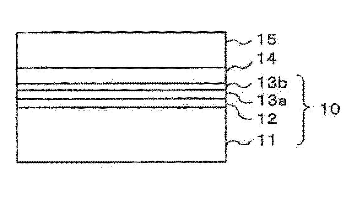
[0122]In the following, the present example will be explained with reference to FIG. 1 and FIG. 3.

[0123]An oxide film and a Pt film are deposited over a 4-inch Si wafer 11 by an electron beam evaporation apparatus and a film 12 having an orientation in (100) is obtained.

[0124]Next, a Pt film 13a of approximately 100 nm having, an orientation in (100) is deposited over the film 12 by a sputtering method.

[0125]Next, a SrRuO3 film 13b having an orientation in (001) is deposited over the Pt film 13a by a sputtering method.

[0126]Successively, a seed crystal film 14 configured with a Pb(Zr, Ti)O3 film is epitaxially grown over this SrRuO3 film 13b by a sputtering method. A sputtering condition at this time is as follows.

[Sputtering Condition]

[0127]Apparatus: RF magnetron sputtering apparatus

[0128]Power: 1,500 W

[0129]Gas: Ar / O2

[0130]Pressure: 0.14 Pa

[0131]Temperature: 600° C.

[0132]Film deposition rate: 0.63 nm / sec

[0133]Film deposition time: 1.3 min

[0134]By the above epitaxial growth, the ...

example 2

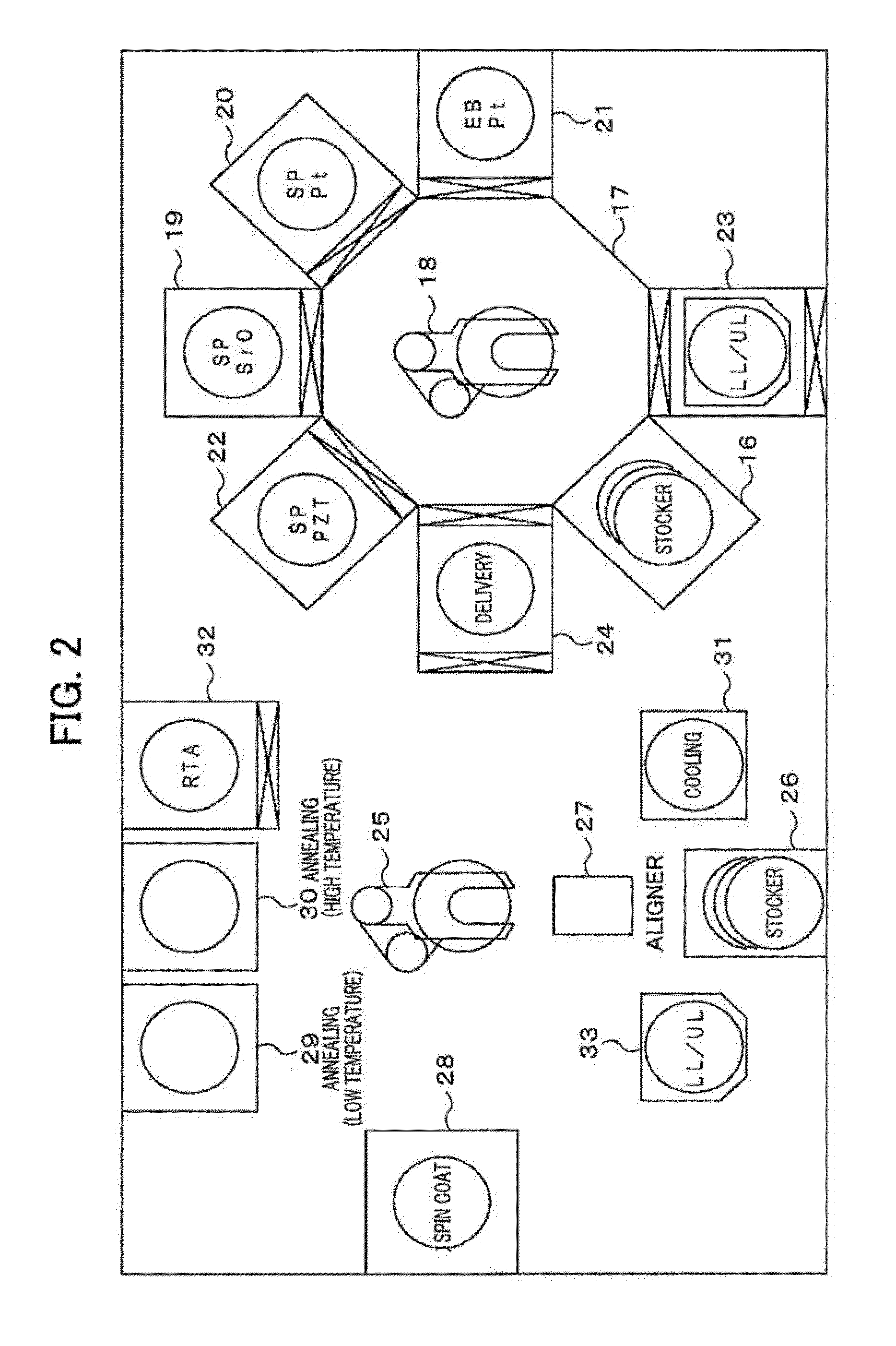
[0149]In the following, the present example will be explained. A ferroelectric crystal film of the present example is deposited by the use of the composite film deposition apparatus shown in FIG. 2.

[0150]A ferroelectric seed crystal film is grown epitaxially on a 4-inch. Si wafer by the same method as that of example 1. The ferroelectric seed crystal film, which is formed in this manner having a thickness of 50 nm, has a single orientation in (001) and has an extremely preferable crystalline property.

[0151]Next, a ferroelectric coated-and-sintered crystal film, which is configured with a PZT thick film having a total thickness of 3.5 μm, is formed overlapping the ferroelectric seed crystal film by spin-coat coating and crystallization under the following condition. Thereby, a sample of the ferroelectric coated-and-sintered crystal film is fabricated, configured with three kinds of film having different compositions; a first layer to a third layer.

[Solution Coating Condition]

[0152]Co...

example 3

[0196]A Pt lower electrode is fabricated over a substrate of 5 nm-TiOx / Si (100) by the use of a DC sputtering apparatus as a film deposition apparatus. A sputtering condition at this time is as follows.

[0197]Substrate temperature: 600° C.

[0198]Growth pressure: 0.3 Pa

[0199]DC power: 200 W

[0200]Sputtering gas: Ar

[0201]Film deposition time: 4 min

[0202]The above deposited Pt lower electrode is a film having a strong orientation only in (111), and this is caused by a strong self orientation property of Pt.

[0203]After that, a seed crystal film configured with a Pb (Zr, Ti)O3 film is epitaxially grown over this Pt lower electrode by a sputtering method. A sputtering condition at this time is as follows.

[Sputtering Condition]

[0204]Apparatus: RF magnetron sputtering apparatus

[0205]Power: 1,500 W

[0206]Gas: Ar / O2

[0207]Pressure: 0.14 Pa

[0208]Temperature: 600° C.

[0209]Film deposition rate: 0.63 nm / sec

[0210]Film deposition time: 1.3 min.

[0211]The seed crystal film which is configured with the Pb...


PUM

PropertyMeasurementUnit
thicknessaaaaaaaaaa
temperatureaaaaaaaaaa
timeaaaaaaaaaa

Abstract

There is provided a manufacturing method of a ferroelectric crystal film in which an orientation of a seed crystal film is transferred preferably and a film deposition rate is suitable for volume production.
A seed crystal film is formed on a substrate in epitaxial growth by a sputtering method, an amorphous film including ferroelectric material is formed over the seed crystal film by a spin-coat coating method, the seed crystal film and the amorphous film are heated in an oxygen atmosphere for oxidation and crystallization of the amorphous film, and thereby a ferroelectric coated-and-sintered crystal film is formed.

Description

BACKGROUND OF THE INVENTION[0001]1. Field of the Invention[0002]The present invention relates to a ferroelectric crystal film including a seed crystal film, an electronic component, a manufacturing method of the ferroelectric crystal film, and a manufacturing apparatus therefor.[0003]2. Description of a Related Art[0004]<Manufacturing Method of a Ferroelectric Crystal Film Using Epitaxial Growth>[0005]FIG. 12 is a cross-sectional view for explaining a conventional manufacturing method of a ferroelectric crystal film.[0006]A Pt film 102 having an orientation in (100) is formed over a substrate 101 such as a 4-inch wafer. Successively, a Pb(Zr, Ti)O3 film (hereinafter, called a “FZT film”) 103 is grown epitaxially over this Pt film 102 by a sputtering method. An example of the sputtering condition at this time is as follows.[Sputtering Condition][0007]Apparatus: RF magnetron sputtering apparatus[0008]Power: 1,500 W[0009]Gas Ar / O2 [0010]Pressure: 0.14 Pa[0011]Temperature: 600° C....

Claims


Application Information

Patent Timeline
Patent Type & Authority Applications(United States)
IPC IPC(8): C30B1/02C30B23/08C30B29/22C30B29/68
CPCC30B1/023C30B29/68C30B23/08C30B29/22C30B7/06C30B23/02Y10T117/10H10N30/079H10N30/078
Inventor KIJIMA, TAKESHIHONDA, YUUJIIITSUKA, DAISUKEHATA, KENJIROU
Owner SAE MAGNETICS (HK) LTD
Why Eureka
Try Eureka