MEMS pressure sensor and manufacturing method therefor

a technology of pressure sensor and manufacturing method, applied in the field of micro electromechanical systems, can solve the problems of high cost and large size, and achieve the effects of reducing the size of the device, avoiding the complexity of packaging process integration, and reducing the cos

Active Publication Date: 2014-01-02
MEMSEN ELECTRONICS
View PDF7 Cites 25 Cited by
  • Summary
  • Abstract
  • Description
  • Claims
  • Application Information

AI Technical Summary

Benefits of technology

[0009]An object of the present invention is to provide a MEMS pressure sensor and a manufacturing method thereof, which can be compatible with the IC manufacturing process, effectively decrease the manufacturing cost and reduce the size of the sensor.
[0056]As compared to the existing technology, the above technical solution has the following advantages.
[0057]The MEMS pressure sensor and the manufacturing method thereof according to the embodiment of the present invention include two substrates, the first substrate is configured to form the piezoresistive pressure sensing unit, and the second substrate is configured to form the conductor connecting layer (and the signal processing circuit). The two substrates are face to face coupled together through the first bonding layer and the second bonding layer, and a sealed structure is formed between the two substrates. Then the back surface of the first substrate is etched by the silicon deep reactive etching, and the sensitive diaphragm element of the piezoresistive pressure sensing unit and the wire-bonding pad area on the second substrate are exposed at the same time. The packaging is performed finally. Therefore, the first substrate and the second substrate may be manufactured separately, and either of the manufacturing processes for the two substrates is compatible with the IC. The two substrates are integrated together through the bonding process, which avoids the complexity of the packaging process integration, decreases the size of a device and reduces the cost, and has the advantage that the process is simple and convenient.
[0058]Furthermore, the above method may be achieved by various kinds of plastic packaging such as QFN, DFN or SOIC. As compared to the manufacturing process for the traditional pressure sensor, the above method may effectively reduce the cost and decrease the size of the sensor.

Problems solved by technology

However, the problem is that, in the above manufacturing and packaging method for the traditional MEMS pressure sensor, the pressure sensor chip and the signal processing circuit chip are discrete chips and integrated together by a packaging process.
The process for the cavity packaging with the plastic cover or a metal cover is complicated and thus not easily compatible with the mature integrated circuit (IC) manufacturing technology, leading to a higher cost and a larger size.

Method used


Image

  • MEMS pressure sensor and manufacturing method therefor
  • MEMS pressure sensor and manufacturing method therefor
  • MEMS pressure sensor and manufacturing method therefor

Examples


first embodiment

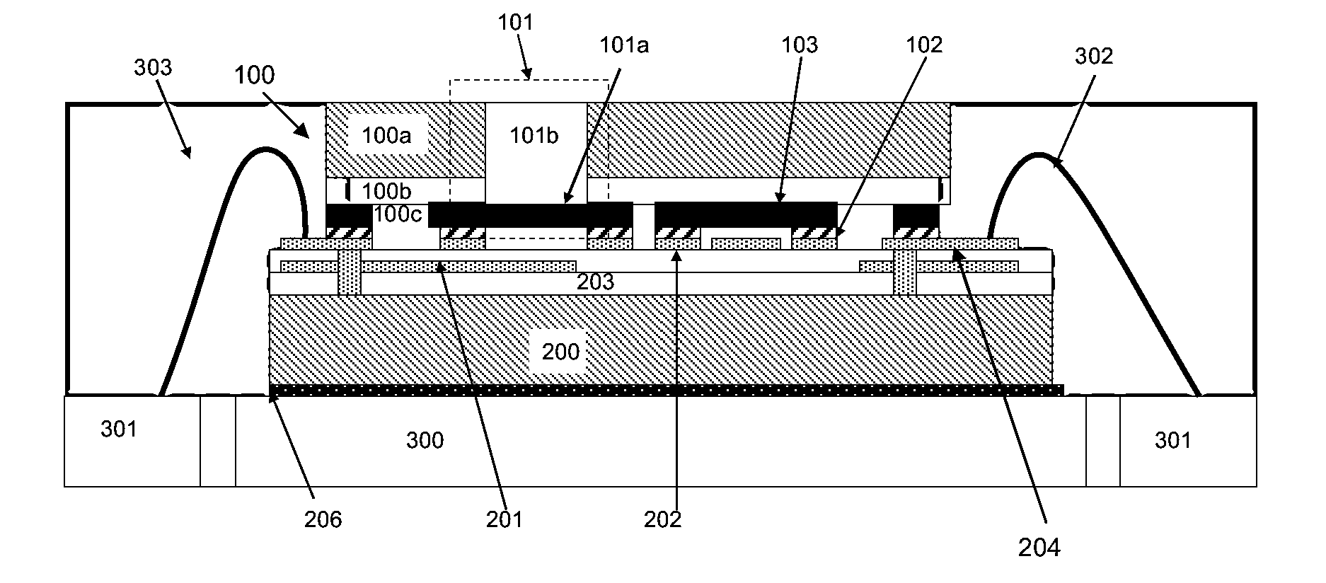
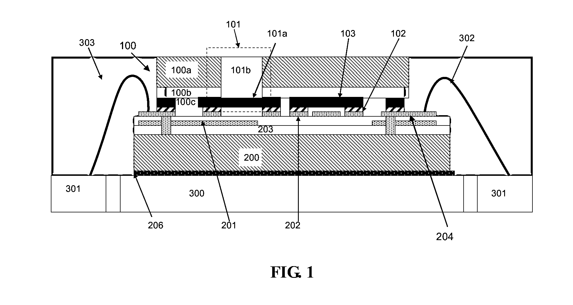
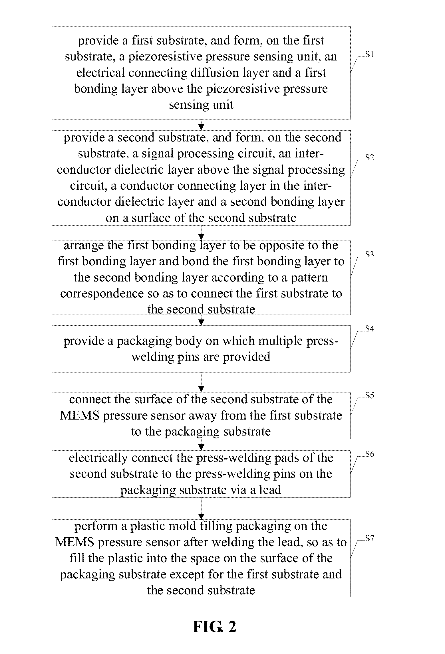
[0067]FIG. 1 is a schematic structural diagram of a MEMS pressure sensor according to the embodiment. As shown, the MEMS pressure sensor includes: a first substrate 100 provided with a piezoresistive pressure sensing unit 101, an electrical connecting diffusion layer 103 and a first bonding layer 102 on a surface of the first substrate 100; and a second substrate 200 provided with an inter-conductor dielectric layer, a conductor connecting layer 201 in the inter-conductor dielectric layer and a second bonding layer 202 on a surface of the second substrate 200.

[0068]The second substrate 200 is arranged opposite to the first substrate 100, the two substrates are fixedly coupled to each other through the first bonding layer 102 and the second bonding layer 202 either of which is formed of a conductive material, and there exists a pattern correspondence between the first bonding layer 102 and the second bonding layer 202. The “pattern correspondence” here means the alignment of the patt...

second embodiment

[0111]FIG. 8 is a schematic structural diagram of the MEMS pressure sensor according to the present embodiment.

[0112]As shown, a self-test electrode 205 is provided on the surface of the second substrate 200 within the reference pressure cavity 101c. The self-test electrode 205 is separated from the sensitive diaphragm 101a at a distance. The self-test electrode 205 corresponds to the sensitive diaphragm in the first substrate 100. And the self-test electrode 205 is coupled to the conductor connecting layer below. A test voltage is applied between the self-test electrode 205 and the sensitive diaphragm 101a so as to achieve the self-test function of the piezoresistive pressure sensing unit. Other structures of the MEMS pressure sensor according to the present embodiment are the same as those of the first Embodiment, and thus omitted here.

[0113]The manufacturing method of the MEMS pressure sensor of this embodiment is different from that of the first embodiment only in that: accordin...


PUM

PropertyMeasurementUnit
temperatureaaaaaaaaaa
conductiveaaaaaaaaaa
pressureaaaaaaaaaa

Abstract

An MEMS pressure sensor comprising: a first substrate (100) having a sensing diaphragm (101a) of a piezoelectric pressure sensing unit (101), an electrical connection diffusion layer (103), and a first bonding layer (102) on a surface of the first substrate (100), a second substrate (200) having an inter-conductor dielectric layer (203), a conductor connection layer (201) arranged within the inter-conductor dielectric layer (203), and a second bonding layer (202) on a surface of the second substrate (200). The second substrate (200) and the first substrate (100) are oppositely arranged, and are fixedly coupled via the first bonding layer (102) and the second bonding layer (202); the first bonding layer (102) and the second bonding layer (202) have matching patterns and are both made from a conductive material. Also provided is a method for manufacturing the MEMS pressure sensor. The MEMS pressure sensor and the manufacturing method therefore allow for compatibility with integrated circuit manufacturing technique, for effectively reduced manufacturing costs, and for a downsized sensor.

Description

[0001]This application claims the priority to the Chinese patent application No. 201110061456.5, entitled “MEMS PRESSURE SENSOR AND MANUFACTURING METHOD THEREOF”, filed with the State Intellectual Property Office of PRC on Mar. 15, 2011, which is incorporated herein by reference in its entirety.FIELD OF THE INVENTION[0002]The present invention relates to the technical field of Micro Electromechanical System (MEMS), and particularly to a MEMS pressure sensor and a manufacturing method thereof.BACKGROUND OF THE INVENTION[0003]MEMS is a micro electromechanical system which integrates a micro sensor, an executer and a signal processing and controlling circuit, an interface circuit, communication and a power supply as a whole. In recent years, the traditional mechanical sensor is progressively replaced by the MEMS pressure sensor in the fields of automotive electronics, consumer electronics and industry electronics, and the MEMS pressure sensor has broad market prospects. For example, th...

Claims


Application Information

Patent Timeline
Patent Type & Authority Applications(United States)
IPC IPC(8): B81B3/00B81C1/00
CPCB81B3/0021B81C1/00158B81B2201/0264B81B2207/012B81C2203/0154B81C2203/0792G01L9/0042G01L9/0054B81C1/00238
Inventor LIU, LIANJUN
Owner MEMSEN ELECTRONICS
Why Eureka
Try Eureka