I-shaped gate electrode for improved sub-threshold mosfet performance

a technology of mos transistor and gate electrode, which is applied in the field of integrated circuits, can solve the problems of high flicker noise, low efficiency, and low efficiency of mos transistor, and achieve the effect of improving the performance of sub-threshold mos transistors and reducing the risk of mos transistor flicker nois

Inactive Publication Date: 2014-04-17
TEXAS INSTR INC
View PDF4 Cites 23 Cited by
  • Summary
  • Abstract
  • Description
  • Claims
  • Application Information

AI Technical Summary

Benefits of technology

[0016]Embodiments of this invention provide a transistor structure and method of manufacturing the same that avoids subthreshold conduction degradation due to gate dielectric thinning and other mechanisms at the active-to-isolation structure interface of the transistor channel edge.

Problems solved by technology

Subthreshold leakage current, which is the drain current conducted by a MOS transistor under drain-to-source bias but at gate voltages below the threshold voltage, is generally undesirable in digital circuits, particularly in applications that are sensitive to power consumption, such as mobile devices, implantable medical devices, and other battery-powered systems.
MOS transistor flicker noise appears as deviations of circuit performance from design.
It has been observed that analog circuits with subthreshold-biased MOS transistors are especially susceptible to flicker noise.
Analog circuits constructed with transistors with lower conduction threshold at channel edges due to this mechanism also exhibit a high level of flicker noise, especially at low gate voltage and with applied back bias.
This large device-to-device variance is somewhat inherent due to nature of this mechanism, in which a significant fraction of the subthreshold channel current is conducting at the poorly controlled channel edge of interface IF.
Processes such as chemical-mechanical planarization (CMP) and wet oxide etch typically have a high process variation, randomize the INWE mechanism and thus cause significant mismatch among the transistors in a given integrated circuit.
This device mismatch is especially problematic in those analog circuits that rely on good matching of device characteristics, such as low power bandgap voltage reference circuits, as described in Joly et al., “Temperature and Hump Effect Impact on Output Voltage Spread of Low Power Bandgap Designed in the Sub-threshold Area”, International Symposium on Circuits and Systems (IEEE, May 2011), pp.
However, fabrication of such a dual gate dielectric structure is significantly more complicated than that for a gate dielectric of a single thickness, involving at least one additional photolithography process as well as an additional etch.
Both of the additional lithography and etch processes, besides adding manufacturing cost, also increase process variability among transistors in the same integrated circuit, and from wafer to wafer.
In many situations, it is in fact difficult to control the extension of the fence into the active region, which is especially costly as the tolerance and controllability of the fence becomes a significant fraction of the active area.
As such, the thicker dielectric fence approach is generally not useful at deep submicron widths.
However, it has been observed that fabrication of ring-shaped gate structure 8′ is quite difficult, in that the dimensions of polysilicon structures of this shape are not as well-controlled as orthogonal rectangular shapes.
Furthermore, it is difficult to derive compact computer models for current conduction in ring-FETs, and those models are not scalable, restricting the flexibility with which variable widths and lengths of MOSFETS can be used during circuit design.

Method used


Image

  • I-shaped gate electrode for improved sub-threshold mosfet performance
  • I-shaped gate electrode for improved sub-threshold mosfet performance
  • I-shaped gate electrode for improved sub-threshold mosfet performance

Examples


Embodiment Construction

[0026]This invention will be described in connection with its embodiments, namely as implemented into an integrated circuit including metal-oxide-semiconductor (MOS) transistors, as it is contemplated that the invention will be especially beneficial in such an implementation. However, it is contemplated that this invention can provide significant benefit when applied to many other integrated circuit structures and methods. Accordingly, it is to be understood that the following description is provided by way of example only, and is not intended to limit the true scope of this invention as claimed.

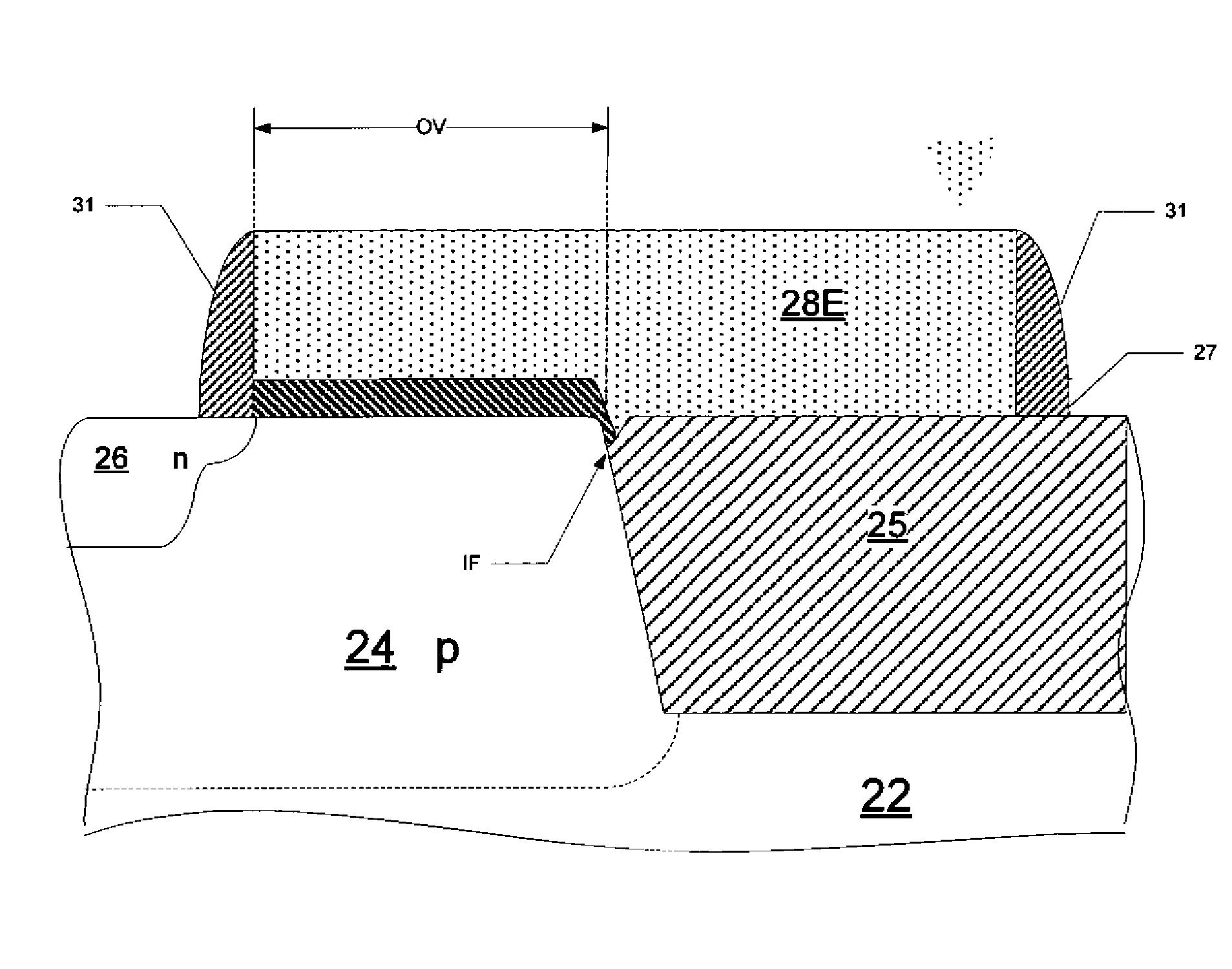
[0027]FIGS. 2a and 2b illustrate in plan view, and FIGS. 2c and 2d in cross-sectional views, the construction of transistor 20 according to embodiments of this invention. In this example, transistor 20 is a metal-oxide semiconductor (MOS) transistor formed at a selected location of the surface of single-crystal silicon substrate 22. More specifically, transistor 20 is an n-channel MOS transi...


PUM


Abstract

Metal-oxide-semiconductor (MOS) transistors with reduced subthreshold conduction, and methods of fabricating the same. Transistor gate structures are fabricated in these transistors of a shape and dimension as to overlap onto the active region from the interface between isolation dielectric structures and the transistor active areas. Minimum channel length conduction is therefore not available at the isolation-to-active interface, but rather the channel length along that interface is substantially lengthened, reducing off-state conduction.

Description

CROSS-REFERENCE TO RELATED APPLICATIONS[0001]Not applicable.STATEMENT REGARDING FEDERALLY SPONSORED RESEARCH OR DEVELOPMENT[0002]Not applicable.BACKGROUND OF THE INVENTION[0003]This invention is in the field of integrated circuits. Embodiments of this invention are more specifically directed to metal-oxide-semiconductor (MOS) transistors.[0004]Many modern electronic devices and systems now include substantial computational capability for controlling and managing a wide range of functions and useful applications. As is fundamental in the art, reduction in the size of physical feature sizes of structures realizing transistors and other solid-state devices enables greater integration of more circuit functions per unit “chip” area, or conversely, smaller chip area consumed for a given circuit function. The capability of integrated circuits for a given cost has greatly increased as a result of this miniaturization trend.[0005]As is fundamental in the art, a MOS transistor ideally conduct...

Claims


Application Information

Patent Timeline
Patent Type & Authority Applications(United States)
IPC IPC(8): H01L29/78H01L21/336
CPCH01L21/28123H01L21/823828H01L29/4238H01L29/7833H01L21/31051H01L21/76224H01L29/0649H01L29/0847H01L29/42356H01L29/42376H01L29/4916H01L29/495H01L29/4966H01L29/66568
Inventor CHATTERJEE, AMITAVA
Owner TEXAS INSTR INC
Why Eureka
Try Eureka