
Gas Barrier Film and Electronic Device

a technology of gas barrier film and electrode film, which is applied in the direction of metallic material coating process, synthetic resin layered products, packaging, etc., can solve the problems of disconnections or short circuits in electrode films, poor gas barrier properties of transparent resin films, and inability to adequately prevent water vapor entry, etc., to achieve high surface flatness, facilitate handling, inhibit layer separation

Active Publication Date: 2014-06-05
LINTEC CORP
View PDF3 Cites 1 Cited by
  • Summary
  • Abstract
  • Description
  • Claims
  • Application Information

AI Technical Summary

Benefits of technology

The gas barrier film described in this patent prevents air and water vapor from entering electronic devices, improving their durability and weather resistance. The film has a smooth surface, reducing the likelihood of short circuits and disconnections. The inorganic material layer and the polyorganosiloxane-based compound layer are securely adhered, ensuring the gas barrier properties are maintained over a long period of time. The gas barrier film is easy to handle and can be applied to processing apparatuses with small diameters.

Problems solved by technology

However, transparent resin films have poor gas barrier properties in comparison with glass substrates, and are unable to adequately prevent entrance of water vapor into solar modules as is.
In addition, since transparent resin films have low surface flatness, when an electrode film is deposited on the surface thereof, protrusions that cause disconnections or short circuits are formed in the electrode film.
In addition, the inorganic thin film is subject to the occurrence of cracking when the gas barrier films are bent, thereby resulting in the risk of gas easily permeating the film at locations where cracking has occurred.
However, in addition the production process of this film being complex, adhesion between the inorganic thin film and organic thin film is low, thereby resulting in increased susceptibility to separation of the thin films.

Method used


Image

  • Gas Barrier Film and Electronic Device
  • Gas Barrier Film and Electronic Device
  • Gas Barrier Film and Electronic Device

Examples


example 1

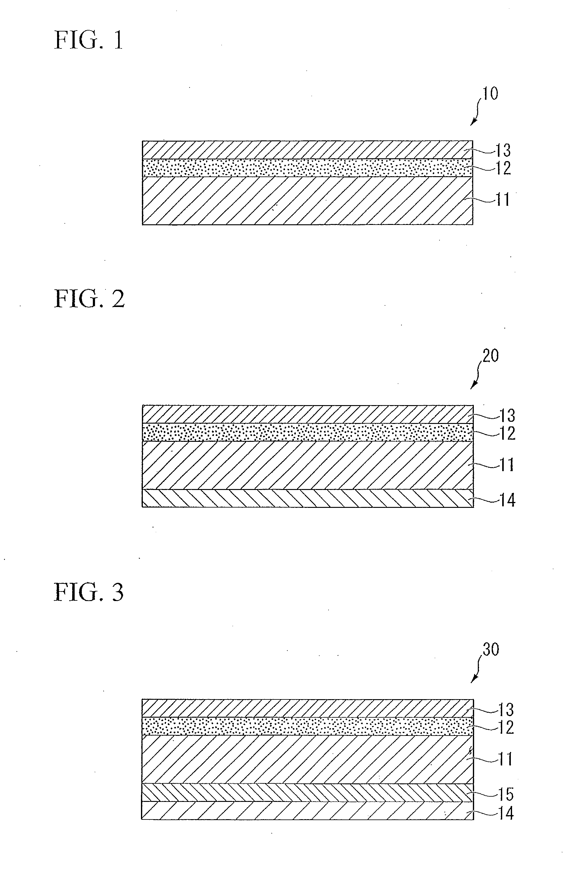
[0135]A polyethylene terephthalate film (produced by Mitsubishi Plastics, Inc., trade name: PET38 T-100) having a thickness of 38 μm was prepared for use as a base.

[0136]Next, a silicone resin (produced by Shin-Etsu Chemical Co., Ltd., trade name: KS847H), mainly composed of polydimethylsiloxane for the polyorganosiloxane-based compound, was coated onto the surface of the base and dried to obtain a polydimethylsiloxane layer (polyorganosiloxane layer) having a thickness of 100 nm.

[0137]Next, a silicon nitride (Si—N) film (inorganic material layer) was deposited on the polydimethylsiloxane layer by dynamic ion mixing method using a sputtering method.

[0138]The conditions of dynamic ion mixing method are indicated below.

[0139]Plasma-forming gas: Mixed gas of argon and nitrogen

[0140]Target: Silicon

[0141]Plasma-forming gas flow rates: argon: 100 cm3 / min (atmospheric pressure: 1.013 hPa, 25° C.), nitrogen: 60 cm3 / min (atmospheric pressure 1.013 hPa, 25° C.)

[0142](Radio Frequency Electrica...

example 2

[0154]A gas barrier film was produced in the same manner as Example 1 with the exception of using a mixed gas of argon and oxygen for the plasma-forming gas when forming the inorganic material layer, and depositing a silicon oxide (SiO2) film by setting the argon flow rate to 100 sccm and setting the oxygen flow rate to 30 sccm.

example 3

[0155]A gas barrier film was produced in the same manner as Example 1 with the exception of depositing an aluminum nitride (Al—N) film by using aluminum for the target when forming the inorganic material layer.


PUM

PropertyMeasurementUnit
voltageaaaaaaaaaa
thicknessaaaaaaaaaa
thicknessaaaaaaaaaa

Abstract

Disclosed is a gas barrier film, which demonstrates superior gas barrier properties and surface flatness, demonstrates a high degree of adhesion between layers and is resistant to cracking when bent, and an electronic device provided therewith. A gas barrier film (10) of the present invention has a base (11), and a polyorganosiloxane layer (12) and an inorganic material layer (13) sequentially provided on at least one side of the base (11), and the inorganic material layer (13) is deposited by dynamic ion mixing method.

Description

TECHNICAL FIELD[0001]The present invention relates to a gas barrier film and an electronic device provided with that gas barrier film.[0002]The present application claims priority on the basis of Japanese Patent Application No. 2009-083871 filed in Japan on Mar. 31, 2009, the contents of which are incorporated herein by reference.BACKGROUND ART[0003]Transparent resin films have been attempted to be used in recent years as an alternative to glass substrates in applications such as image display elements or solar cell modules accompanying requirements for increased flexibility, lighter weight and reduced thickness.[0004]FIG. 5 is a schematic cross-sectional view showing an example of a solar cell module in which a transparent resin film is used as a protective sheet.[0005]This solar cell module 200 is generally composed of a solar cell 201 composed of crystalline silicon or amorphous silicon and the like, an encapsulant (filler layer) composed of an electrical insulator that seals the...

Claims


Application Information

Patent Timeline
Patent Type & Authority Applications(United States)
IPC IPC(8): B32B27/06H01L31/048B32B33/00C08J7/043C08J7/048
CPCC23C14/024C23C14/345C08J2483/04C23C14/0641C23C14/0652C23C14/08C23C14/3485C08J2367/02Y02E10/50H01L31/049B32B9/007B32B9/045B32B15/08B32B27/08B32B27/28B32B27/281B32B27/283B32B27/286B32B27/288B32B27/308B32B27/32B32B27/34B32B27/36B32B27/365B32B2307/306B32B2307/412B32B2307/538B32B2307/712B32B2307/7242B32B2307/7246B32B2307/732B32B2457/00B32B27/06Y10T428/263Y10T428/265Y10T428/31663C08J7/0423C08J7/048C08J7/043B32B33/00
Inventor HOSHI, SINICHIOKUJI, SHIGETO
Owner LINTEC CORP
Learn More