
Waveguide-based detection system with scanning light source

a detection system and waveguide technology, applied in the field of waveguide-based detection systems with scanning light sources, can solve the problems of limited signal strength, short interaction length between bio-samples, high background or noise, etc., and achieve the effect of simple and cost-effectiv

Active Publication Date: 2014-06-26
LDIP LLC
View PDF6 Cites 80 Cited by
  • Summary
  • Abstract
  • Description
  • Claims
  • Application Information

AI Technical Summary

Benefits of technology

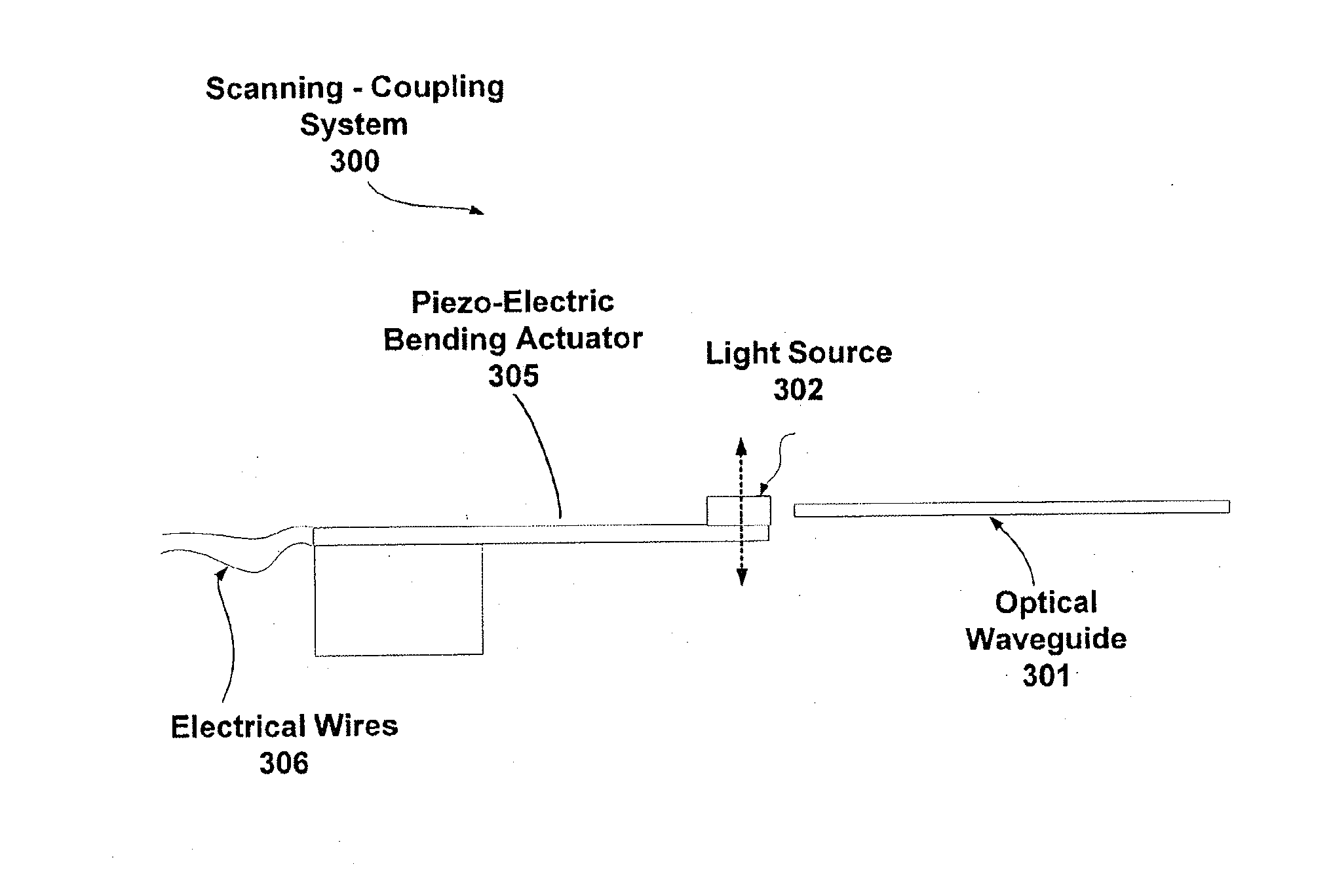
The present invention provides methods and devices to easily and cheaply couple light into optical waveguides. This allows for the simple and cost-effective coupling of multi-wavelength trains of pulses into optical waveguides and the detection of optical signals using a scanning light source. The invention has applications in optical communication and sensing systems.

Problems solved by technology

This arrangement suffers from several inherent limitations including a very short interaction length between the bio-sample and the light (usually a single mono-layer).
This limits the signal strength and thus the SNR.
Another limitation is a high background or noise due to the fact that the back-reflected light and the emitted fluorescent light travel in the same direction.
A further limitation is high sensitivity to both the planarity and the position of the chip that need to be maintained in focus.
Still another limitation is slow operation due to the need to have large enough number of ‘pixels’ (scanned spots) within every sample and long enough integration time.
Yet another limitation is the need for a complicated optical and mechanical structure that entails bulky and expensive systems.
One drawback of this kind of system is relatively poor performance due to uniformity of excitation as well as collection of the light.
This leads to non-repeatable results.
Another drawback is high noise levels due to crosstalk between the different spots.
A further drawback is that large spots and relatively small numbers of elements are required to generate a signal large enough for efficient imaging with the CCD.
Yet another drawback is the long integration time to overcome SNR issues.
The major problems associated with this type of system include non-specificity due to inability to recognize the exact reason for the index change, which may occur from deposition of other material as well as temperature changes.
Another problem is a very slow speed in addressing the different elements which disqualifies this method for running large numbers of element arrays.
This process adds in most of these cases a considerable cost and complexity to the entire system.

Method used


Image

  • Waveguide-based detection system with scanning light source
  • Waveguide-based detection system with scanning light source
  • Waveguide-based detection system with scanning light source

Examples


example 1

Establishing the Limit of Detection

[0373]One feature of the sensors of the current invention is the ability to detect low numbers of biologically active analyte molecules. The following experiments demonstrate this capability. The limit of detection (LOD) of the sensors was determined by measuring fluorescently labeled ovalbumin in solution. The dye used was Alexa Fluor 660; it was excited at 658 nm and emission was measured at 690 nm. All measurements were made at room temperature (25° C.). LOD was assayed using two different methods: 1) determination of the lowest concentration of labeled ovalbumin detectable above buffer background with better than 95% confidence (P<0.05, Student's t-test); and 2) determination of the analytical sensitivity from a standard curve of sensor response vs. concentration (MDL=2*SD / slope, where SD is the standard deviation of the buffer background measurement and slope is the initial slope of the standard curve). These methods are comparable in that bot...

example 2

Detection of Protein-Protein Interactions

[0375]The present invention is useful for measuring protein-protein interactions. In this example, the waveguide-based optical detection technology was used to measure the binding of ovalbumin to anti-ovalbumin antibodies. Before the experiment was conducted, chips with 52.5×4,500 μm sensing elements were dip-coated with anti-ovalbumin antibodies. This procedure involved several steps. First, the chips were cleaned. A chip fabricator coated the active surface of the chips with a thin polymer layer to protect it during wafer dicing. The polymer layer was removed by immersing chips in acetone for 5 minutes, followed by isopropanol for 5 minutes and a second isopropanol rinse for an additional minute. Chips were then washed in deionized water three times and dried in a vacuum desiccator. Next, the surface was activated. To immobilize capture molecules to the waveguides, a thin layer (˜10 nm) of silicon dioxide was created on the chips by Piranha...

example 3

Detection of Polymerization of Nucleic Acids

[0380]The waveguide-based optical detection system can be used to quantify the polymerization of DNA in a primer extension assay. In a primer extension reaction, an mRNA target hybridizes to a DNA primer, and reverse transcriptase uses the mRNA target as a template to add deoxynucleotides (dATP, dTTP, dGTP, dCTP) to the 3′ end of the DNA primer.

[0381]High sensitivity using a waveguide-based optical detection system requires that the hybridization in the primer extension reaction occur at concentrations in the low femtomolar range. Thus, it was first established that hybridization occurs at low concentrations on the surface of the chip. For this experiment, a capture oligonucleotide primer was immobilized to the chip, and a complementary synthetic DNA labeled at the 5′ end with Cy5.5 was incubated with the primer. For experimental rigor, the sequences of both the captured oligonucleotide and a complementary synthetic DNA were verified by ma...


PUM

PropertyMeasurementUnit
widthaaaaaaaaaa
widthaaaaaaaaaa
frequencyaaaaaaaaaa

Abstract

The invention provides methods and devices for generating optical pulses in one or more waveguides using a spatially scanning light source. A detection system, methods of use thereof and kits for detecting a biologically active analyte molecule are also provided. The system includes a scanning light source, a substrate comprising a plurality of waveguides and a plurality of optical sensing sites in optical communication with one or more waveguide of the substrate, a detector that is coupled to and in optical communication with the substrate, and means for spatially translating a light beam emitted from said scanning light source such that the light beam is coupled to and in optical communication with the waveguides of the substrate at some point along its scanning path. The use of a scanning light source allows the coupling of light into the waveguides of the substrate in a simple and cost-effective manner.

Description

CROSS REFERENCE TO RELATED APPLICATIONS[0001]This application is a continuation-in-part of U.S. patent application Ser. No. 12 / 769,364, filed Apr. 28, 2010, titled “WAVEGUIDE-BASED DETECTION SYSTEM WITH SCANNING LIGHT SOURCE,” now U.S. Pat. No. 8,675,199, which claims benefit under 35 U.S.C. §119(e) of U.S. Patent Provisional Application No. 61 / 173,771, filed Apr. 29, 2009, titled “GENERATION OF OPTICAL PULSES IN A WAVEGUIDE USING A SPATIALLY SCANNING LIGHT SOURCE” and U.S. Patent Provisional Application No. 61 / 223,550 filed Jul. 7, 2009 and titled “WAVEGUIDE-BASED DETECTION WITH SCANNING LIGHT SOURCE,” each of which is herein incorporated by reference in its entirety.[0002]U.S. patent application Ser. No. 12 / 769,364 is also a continuation-in-part of U.S. patent application Ser. No. 11 / 683,808, filed Mar. 8, 2007, titled “OPTICAL SCANNING SYSTEM,” now U.S. Pat. No. 7,951,583, which claims benefit under 35 U.S.C. §119(e) of U.S. Patent Provisional Application No. 60 / 743,458, filed Ma...

Claims


Application Information

Patent Timeline
Patent Type & Authority Applications(United States)
IPC IPC(8): G01N21/64G01N33/543
CPCG02B6/4226G01N33/54373G01N21/6486B01L3/502715G01N21/6428G01N21/6454G01N21/648B01L2300/0636B01L2300/0654B01L2300/0816B01L2300/0819Y10T436/143333C12Q1/6825G01N33/56988G01N2021/6439G01N2201/0696G01N2201/08G01N2201/103
Inventor DUER, REUVEN
Owner LDIP LLC
Learn More