Polarization effect carrier generating device structures having compensation doping to reduce leakage current

a carrier generation and polarization effect technology, applied in the field of semiconductor structures, can solve the problems of increasing the leakage current of the device, insufficient thermal energy to create any significant number of electron or hole carriers, and device leakage current, so as to reduce the leakage current, and reduce the resistance of the compensation doped algan layer

Inactive Publication Date: 2014-07-03
RAYTHEON CO
View PDF2 Cites 4 Cited by
  • Summary
  • Abstract
  • Description
  • Claims
  • Application Information

AI Technical Summary

Benefits of technology

[0009]The compensation doped Aluminum Gallium Nitride (AlxGa1-xN) barrier layer is under tensile, elastic strain on the GaN buffer layer thereby again causing piezoelectric charge to form is the top-most portion of the GaN layer. Also at the AlGaN / GaN interface, the difference in the spontaneous polarization of these two materials again results in additional polarization charge in the top-most portion, of the GaN layer. Here, however, for the compensation doped AlxGa1-xN barrier layer, unwanted electric carriers derived from the carrier generating contaminants in the AlxGa1-xN barrier layer are trapped out by the compensation doping therein, resulting hi a much more resistive AlGaN layer and a device having reduced leakage current. The unwanted carriers derived from the carrier generating contaminants in the AlGaN barrier layer are now trapped by the compensation doping. More particularly, the trap atoms (i.e., the compensation dopant) added to the AlxGa1-xN barrier layer capture the electronic charge derived from the carrier generating contaminants in the AlxGa1-xN barrier layer, resulting in a much more resistive AlxGa1-xN barrier layer with reduced leakage current. Consequently an IGFET-like structure is in effect obtained without growing an insulating layer on the AlGaN surface.
[0010]With such an arrangement, the resistivity of the compensation doped AlGaN layer is increased by trapping out or capturing unwanted electronic charge from carrier generating contaminants in the AlGaN barrier layer. With these unwanted electronic carriers eliminated, the device structure will have lower leakage entreats without requiring an insulating layer on the AlGaN surface. Further, the compensation doping in the AlGaN barrier layer does not significantly reduce the carrier concentration in the topmost portion of the GaN layer created by polarization effects.

Problems solved by technology

If the dopant electronic state is more than approximately 10 kT in energy from either the conduction band or valence band, thermal energy is insufficient to create any significant number of electron or hole carriers.
As important issue with polarization device structures such as the GaN HEMT device is device leakage currents.
More particularly, in growing the AlGaN layer there are contaminants in the growth process such as oxygen which can provide unwanted electronic carriers because they have energy levels less than 10 kT from either the conduction band or the valance band of the AlGaN layer.
Under high fields in the device structure, these unwanted carriers (derived from the contaminants) increase the leakage current of the device.
Also charge may be released by defects such as dislocations in the AlGaN layer produced during the growth process.
Conductivity caused by the carrier generating contaminants or crystalline defects which have an energy level within 10 kT of the valence band or conduction band in this layer will result in device leakage resulting in degraded performance such as reduced efficiency and breakdown voltage.
This approach however may not always be desirable because: first, an additional and different material (i.e., the insulator) must now be deposited onto the AlxGa1-xN surface of the GaN HEMT; this insulator material must not degrade or react with the AlxGa1-xN surface at process temperatures; and unless the AlGaN layer is thinned, the gate electrode will be further away from the carriers thereby reducing the transconductance of the device.
Here, however, for the compensation doped AlxGa1-xN barrier layer, unwanted electric carriers derived from the carrier generating contaminants in the AlxGa1-xN barrier layer are trapped out by the compensation doping therein, resulting hi a much more resistive AlGaN layer and a device having reduced leakage current.

Method used


Image

  • Polarization effect carrier generating device structures having compensation doping to reduce leakage current
  • Polarization effect carrier generating device structures having compensation doping to reduce leakage current
  • Polarization effect carrier generating device structures having compensation doping to reduce leakage current

Examples


Embodiment Construction

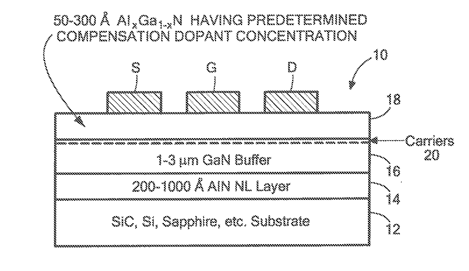
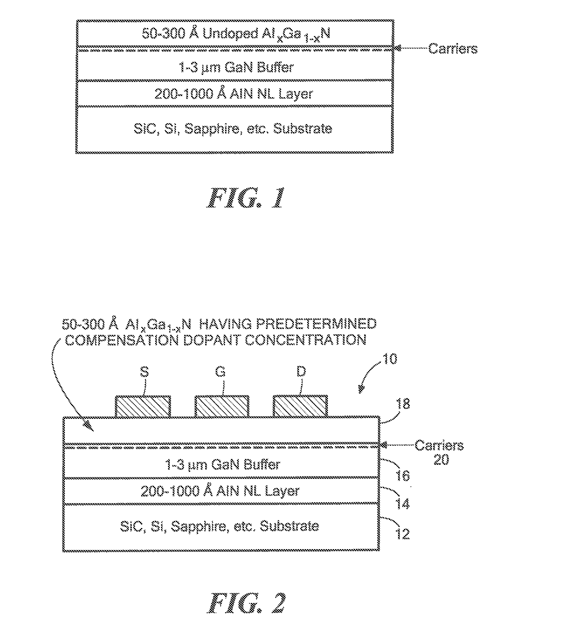
[0032]Referring now to FIG. 2, a HEMT device 10 is shown having a substrate 12, for example, silicon carbide (SiC), silicon (Si) or Sapphire, has a 200 Angstrom to 1000 Angstrom thick, nucleation layer (NL) 14 of Aluminum Nitride (AlN) formed on substrate 12 and a 1-3 micron thick III-V semiconductor buffer layer 16 of here, for example, GaN formed on the AlN layer 14. A 50-300 Angstrom thick layer 18 of here carbon-doped Aluminum Gallium Nitride (AlxGa1-xN) barrier is under tensile, elastic strain on the GaN buffer layer 16 thereby causing piezoelectric polarization charge 20 to form in the top-most portion of the GaN layer 16. Also at the AlGaN / GaN interface, the difference in the spontaneous polarization of these two materials results in additional polarization charge 20 in the top-most portion of the GaN layer 16.

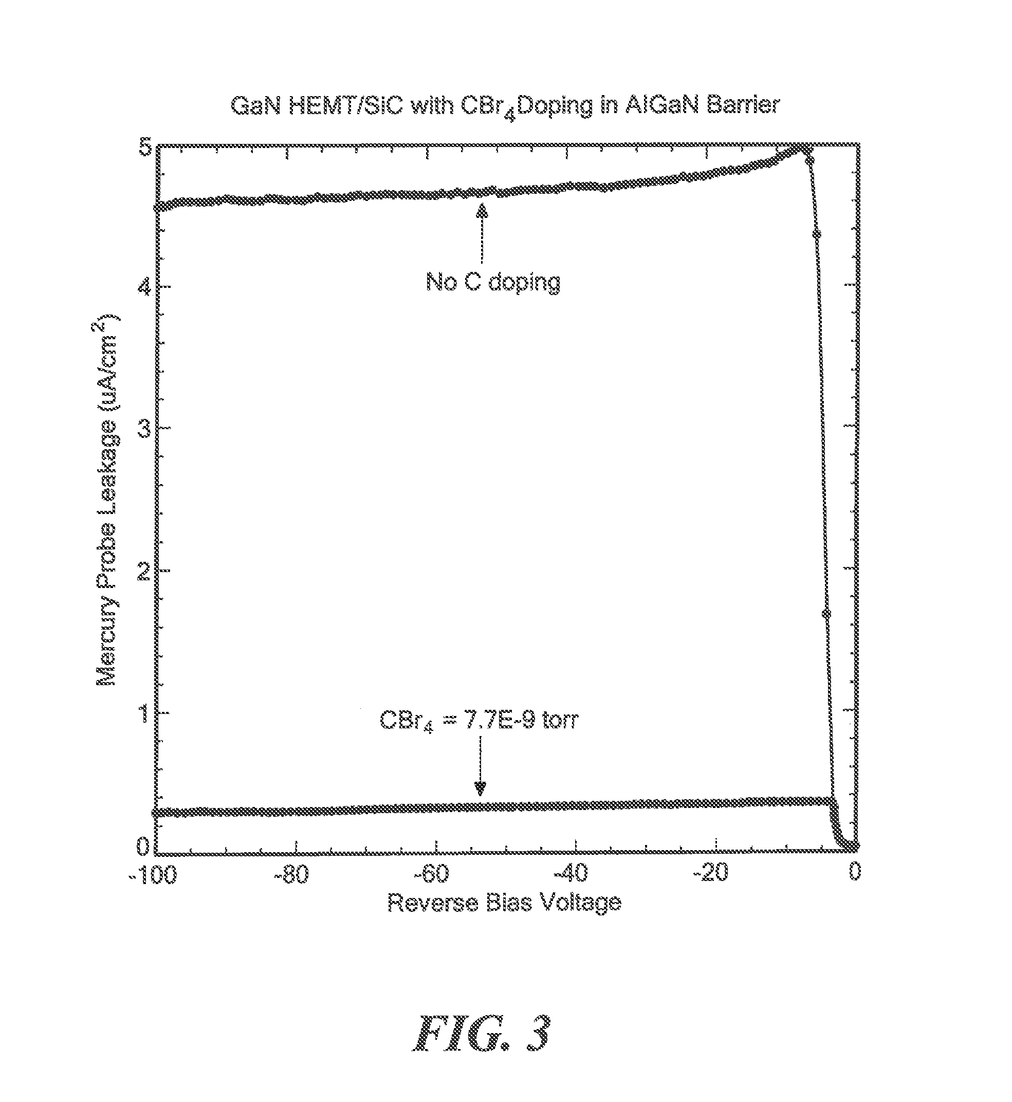
[0033]It should also be noted that during the formation of the AlxGa1-xN barrier layer there may be contaminants having energy levels outside of 10 kT from the valance ...


PUM


Abstract

A semiconductor structure having: a first semiconductor layer; and an electric carrier generating layer disposed on the first semiconductor layer to generate electric carriers within the first semiconductor layer by polarization effects, the electric carrier generating layer having a predetermined conduction band and a predetermined valance band, the electric carrier generating layer having a concentration of non-carrier generating contaminants having an energy level, the difference in the energy level of the non-carrier type contaminants and the energy level of either the conduction band or the valence band being greater than 10 kT, where k is Boltzmann's constant and T is the temperature of the electric carrier generating semiconductor layer, the electric carrier generating semiconductor layer being doped with a dopant having an energy level, the difference in the energy level of the dopant and the energy level of either the conduction band or the valence band being greater than 10 kT, the dopant having a concentration equal to or greater than the concentration of the non-carrier generating contaminants.

Description

TECHNICAL FIELD[0001]This disclosure relates generally to semiconductor structures and more particularly to semiconductor structures wherein mobile electric carriers are generated through polarization effects.BACKGROUND AND SUMMARY[0002]As is known is the art, in solid state physics, a band gap, also called an energy gap or bandgap, is an energy range in a pure crystalline solid where no electronic states can exist. In graphs of the electronic band structure of such crystalline solids the band gap generally refers to the energy difference (in electron volts, eV) between the top of the valence band and the bottom of the conduction band is insulators and semiconductors. In many semiconductor devices, such as in transistor devices, dopants are incorporated into the crystal which create electronic states inside the bandgap. If the energy of the electronic state is within approximately kT of the conduction band, where k is Boltzmann's constant and T is the temperature of the semiconducto...

Claims


Application Information

Patent Timeline
Patent Type & Authority Applications(United States)
IPC IPC(8): H01L29/20
CPCH01L29/2003H01L29/207H01L29/66462H01L29/7787
Inventor HOKE, WILLIAM E.
Owner RAYTHEON CO
Why Eureka
Try Eureka