Enhanced Optical Gain and Lasing in Indirect Gap Semiconductor Thin Films and Nanostructures

a thin film, indirect gap technology, applied in the direction of laser optical resonator construction, semiconductor lasers, lasers, etc., can solve the problems of significantly lower quantum efficiency, impractical threshold current density values, and the inability to use widely used materials

Active Publication Date: 2014-07-03
JAIN FAQUIR C
View PDF4 Cites 33 Cited by
  • Summary
  • Abstract
  • Description
  • Claims
  • Application Information

AI Technical Summary

Problems solved by technology

Unfortunately, this precludes using widely used materials such as Si (the mainstay of integrated circuit industry), Ge, GaP, and other compound semiconductors for fabrication.
It should be appreciated that light emission in indirect energy gap semiconductors, such as Silicon, gallium phosphide (GaP) and other indirect energy gap materials, exhibit significantly lower quantum efficiency ηq and, hence, optical gain when p-n junctions are configured as lasers and result in impractical threshold current density values.
Unfortunately, the limitations associated with band-filling and tensile-strained Ge structures have not resulted in lasers with acceptable threshold current densities from practical on-chip integration perspective.
However, the threshold current density is very high in this type of system, and as a result one has to operate at lower temperatures (below 77K) to obtain stimulated emission.
This is attributed to the lack of appropriate quantum well barrier heights (or offsets) for electrons (ΔEc) and holes (ΔEv) in the conduction and valence band, respectively.

Method used


Image

  • Enhanced Optical Gain and Lasing in Indirect Gap Semiconductor Thin Films and Nanostructures
  • Enhanced Optical Gain and Lasing in Indirect Gap Semiconductor Thin Films and Nanostructures
  • Enhanced Optical Gain and Lasing in Indirect Gap Semiconductor Thin Films and Nanostructures

Examples


Embodiment Construction

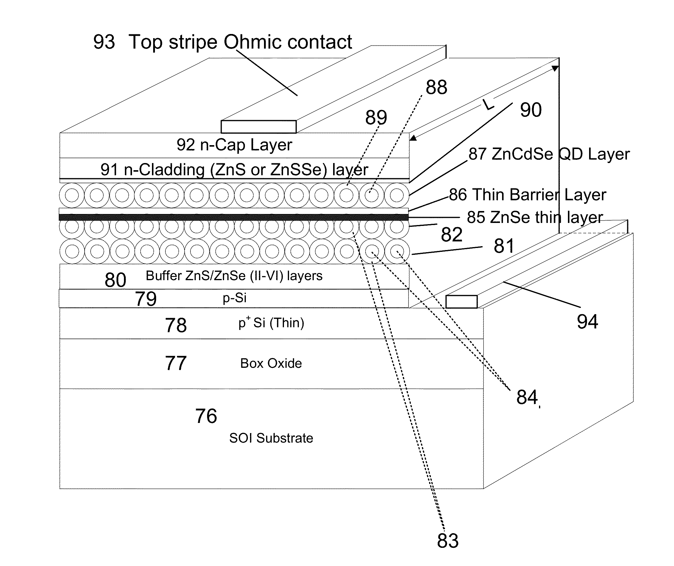
[0033]It should be appreciated that in accordance with the present invention, the figures describe hereinabove involve edge-emitting laser structures with resonant cavity configuration. Surface-emitting structures are also envisioned using disclosed active layers with appropriate spacer and quarter wave dielectric mirrors. The spacer and mirror layers are envisioned to be implemented using barrier materials and / or cladding materials. Distributed feedback (DFB) configurations in edge-emitting and vertical cavity surface emitting laser (VCSEL) are also envisioned using the active layer, cladding layers, and substrates disclosed in here.

[0034]The present invention includes light-emitting and lasing structures that use Ge, SiGe, Si, GaAsP, GaP, and other indirect gap semiconductors. Structures facilitating creation of excitonic transitions which yield higher internal quantum efficiency in generating photons are described. Excitons are envisioned in structures including: (1) two differen...


PUM


Abstract

Structures and methodologies to obtain lasing in indirect gap semiconductors such as Ge and Si are provided and involves excitonic transitions in the active layer comprising of at least one indirect gap layer. Excitonic density is increased at a given injection current level by increasing their binding energy by the use of quantum wells, wires, and dots with and without strain. Excitons are formed by holes and electrons in two different layers that are either adjacent or separated by a thin barrier layer, where at least one layer confining electrons and holes is comprised of indirect gap semiconductor such as Si and Ge, resulting in high optical gain and lasing using optical and electrical injection pumping. In other embodiment, structures are described where excitons formed in an active layer confining electrons in the direct gap layer and holes in the indirect gap layer; where layers are adjacent or separated by a thin barrier layer. The carrier injection structures are configured as p-n junctions and metal-oxide-semiconductor (MOS) field-effect transistors. The optical cavity is realized to confine photons. In the case of MOS structures, electrons from the inversion layer, formed under the gate at voltages above threshold, are injected into one or more layers comprising of quantum wells (2-d), quantum wires (1-d) and quantum dots (0-d) structures. The confinement of photons emitted upon electron-hole recombination produces lasing in active layer comprising of dots / wells. Bipolar transistor structures can also be configured as lasers.

Description

CROSS REFERENCE TO RELATED APPLICATIONS[0001]This application claims benefit of priority of the filing date of U.S. Provisional Patent Application No. 61 / 747,849 filed Dec. 31, 2012, the contents of which are incorporated herein by reference in its entirety.FIELD OF THE INVENTION[0002]The present invention relates to light-emitting and lasing structures, and more particularly to achieving enhanced optical gain and Lasing in semiconductor thin films and nanostructure materials.BACKGROUND OF THE INVENTION[0003]Lasing in direct energy gap semiconductors has been well known since the 1960s when low-temperature GaAs homojunctions lasers and subsequently room temperature AlGaAs—GaAs double heterojunction lasers were first reported. This was followed by the development of quantum well, quantum wire and more recently, quantum dot lasers. Both edge-emitting and surface-emitting configurations are also well known in the prior art. Semiconductor lasers are fabricated using direct gap materials...

Claims


Application Information

Patent Timeline
Patent Type & Authority Applications(United States)
IPC IPC(8): H01S5/34
CPCH01S3/30H01S5/021H01S5/06203H01S5/10H01S5/3214H01S5/3403H01S5/3412H01S5/3427H01S5/4025H01S5/2009B82Y20/00
Inventor JAIN, FAQUIR C.
Owner JAIN FAQUIR C
Why Eureka
Try Eureka