Two-sided laser patterning on thin film substrates

a thin film substrate and laser patterning technology, applied in the field of transparent conductors, can solve the problems of inconvenient vacuum deposition process, inconvenient patterning process, and inability to form patterns and circuits,

Inactive Publication Date: 2014-07-24
CHAMP GREAT INTL
View PDF6 Cites 54 Cited by
  • Summary
  • Abstract
  • Description
  • Claims
  • Application Information

AI Technical Summary

Benefits of technology

[0008]There remains a need in the art to pattern transparent conductors in a low-cost, high-throughput process.

Problems solved by technology

However, metal oxide films are fragile and prone to damage during bending or other physical stresses.
Moreover, the process of vacuum deposition is not conducive to forming patterns and circuits.
This typically results in the need for costly patterning processes such as photolithography.
In addition, a metal oxide film tends to have trouble properly adhering to certain substrates that are prone to adsorbing moisture, such as plastic and organic substrates (e.g., polycarbonates).
Applications of metal oxide films on these flexible substrates are therefore severely limited.

Method used


Image

  • Two-sided laser patterning on thin film substrates
  • Two-sided laser patterning on thin film substrates
  • Two-sided laser patterning on thin film substrates

Examples


Embodiment Construction

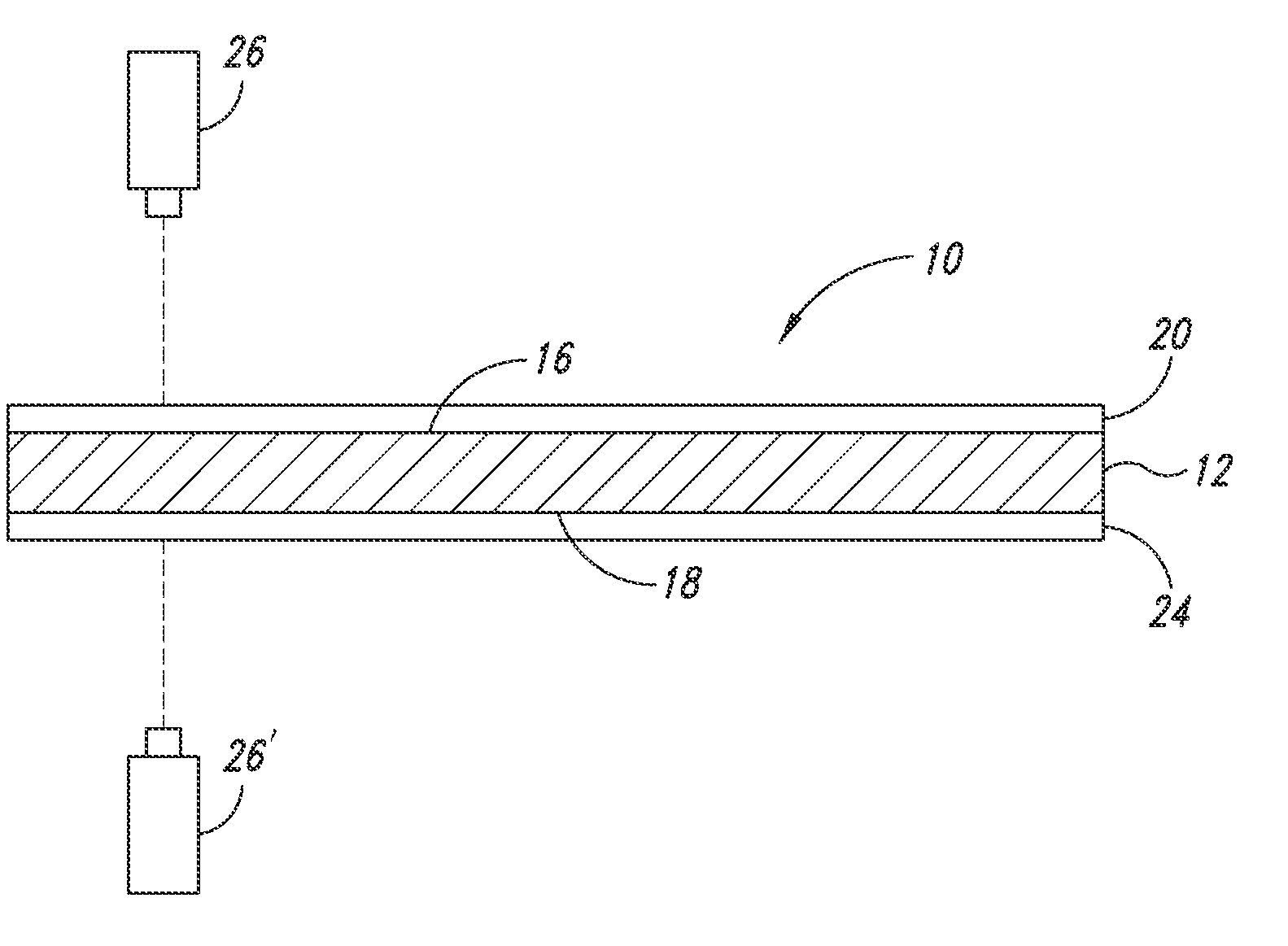
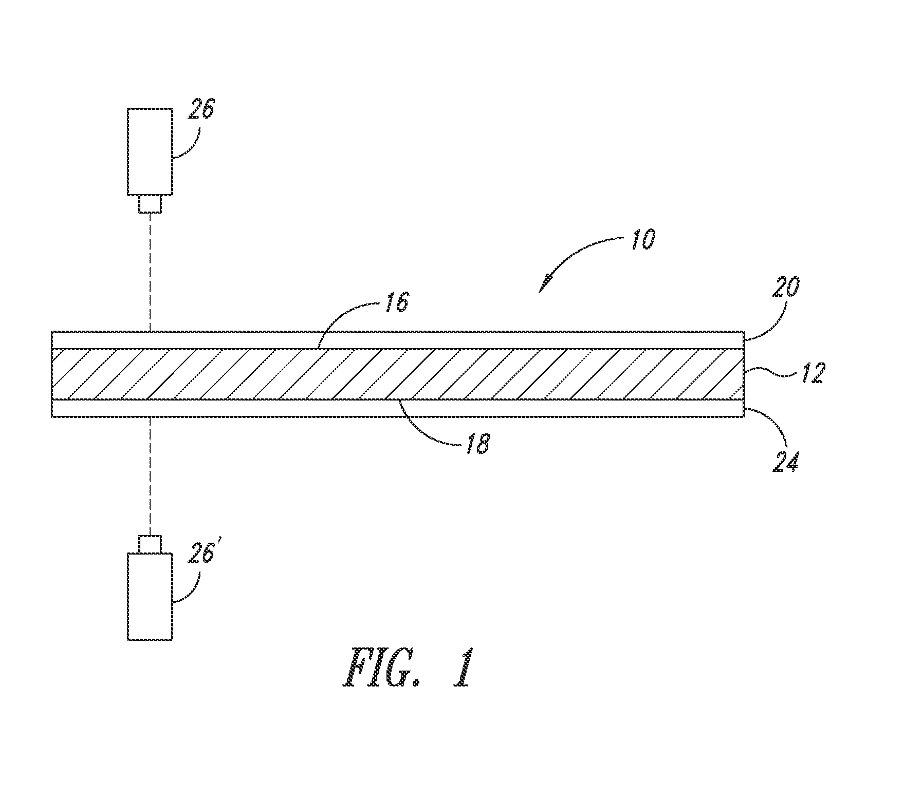
[0024]Described herein are transparent conductors and methods of patterning the same. The patterned transparent conductors are particularly suitable as transparent electrodes in a wide variety of devices including, without limitation, display devices (e.g., touch screens, liquid crystal displays, plasma display panels and the like), electroluminescent devices such as OLED devices, and photovoltaic cells.

[0025]As used herein, “patterning” broadly refers to a process that creates conductive features (e.g., lines or traces) demarcated by electrically insulating regions on the surface of a substrate. A pattern does not necessarily have repeating or regular features; rather, a pattern can simply be an arrangement in which any one conductive feature (e.g., conductive line) is electrically isolated from another conductive feature by one or more insulating regions.

[0026]Nevertheless, many applications of the patterned transparent conductors require regularly spaced conductive lines of subst...


PUM

PropertyMeasurementUnit
blocking wavelengthsaaaaaaaaaa
specific wavelengthsaaaaaaaaaa

Abstract

Disclosed herein are double-sided transparent conductive films suitable for patterning by laser ablation.

Description

BACKGROUND[0001]1. Technical Field[0002]This invention is related to transparent conductors, methods of patterning the same, and applications thereof.[0003]2. Description of the Related Art[0004]Transparent conductors refer to thin conductive films coated on high-transmittance surfaces or substrates. Transparent conductors may be manufactured to have surface conductivity while maintaining reasonable optical transparency. Such surface conducting transparent conductors are widely used as transparent electrodes in flat liquid crystal displays, touch panels, electroluminescent devices, and thin film photovoltaic cells; as anti-static layers; and as electromagnetic wave shielding layers.[0005]Currently, vacuum deposited metal oxides, such as indium tin oxide (ITO), are the industry standard materials for providing optical transparency and electrical conductivity to dielectric surfaces such as glass and polymeric films. However, metal oxide films are fragile and prone to damage during ben...

Claims


Application Information

Patent Timeline
Patent Type & Authority Applications(United States)
IPC IPC(8): H05K1/02H05K3/02
CPCH05K3/027H05K1/0274B23K26/0006B23K26/18B23K26/0619B23K26/355B23K2101/34B23K2101/40B23K2103/56G06F2203/04103H01L31/1884H05K1/0326H05K1/0393H05K1/097H05K1/144H05K2201/0108H05K2201/0112H05K2201/0145H05K2201/015H05K2201/0154H05K2201/0158H05K2201/0162H05K2201/026H05K2201/043H05K2203/108H05K2203/1142H05K2203/1572Y02E10/50
Inventor JONES, DAVIDMANSKY, PAULSPAID, MICHAEL A.
Owner CHAMP GREAT INTL
Why Eureka
Try Eureka