Composite Substrate and Method for Manufacturing the Same

Active Publication Date: 2014-07-31
NGK INSULATORS LTD +1
4 Cites 6 Cited by

AI-Extracted Technical Summary

Problems solved by technology

A piezoelectric substrate, such as an LT or LN substrate, has a large electromechanical coupling coefficient and is therefore advantageous for achieving filter characteristics over a wide band, although this substrate is disadvantageous in that it ha...

Benefits of technology

[0028]In step (e), the piezoelectric substrate is polished to a predetermined thickness (for example, 10 to 50 μm), and the two substrates are then annealed at a temperature higher than 200° C. This reduces thermal stress and also improves the adhesion strength between the two substrates. The annealing temp...

Abstract

The present invention provides a composite substrate comprising a piezoelectric substrate that is a single-crystal lithium tantalate or lithium niobate substrate, a support substrate that is a single-crystal silicon substrate, and an amorphous layer containing argon and joining together the piezoelectric substrate and the support substrate. The amorphous layer includes, in order from the piezoelectric substrate toward the composite substrate, a first layer, a second layer, and a third layer. The first layer contains a larger amount of a constituent element of the piezoelectric substrate than the second and third layers, the third layer contains a larger amount of a constituent element of the support substrate than the first and second layers, and the second layer contains a larger amount of argon than the first and third layers.

Application Domain

Technology Topic

Secondary layerComposite substrate +6

Image

  • Composite Substrate and Method for Manufacturing the Same
  • Composite Substrate and Method for Manufacturing the Same
  • Composite Substrate and Method for Manufacturing the Same

Examples

  • Experimental program(7)

Example

Example 1
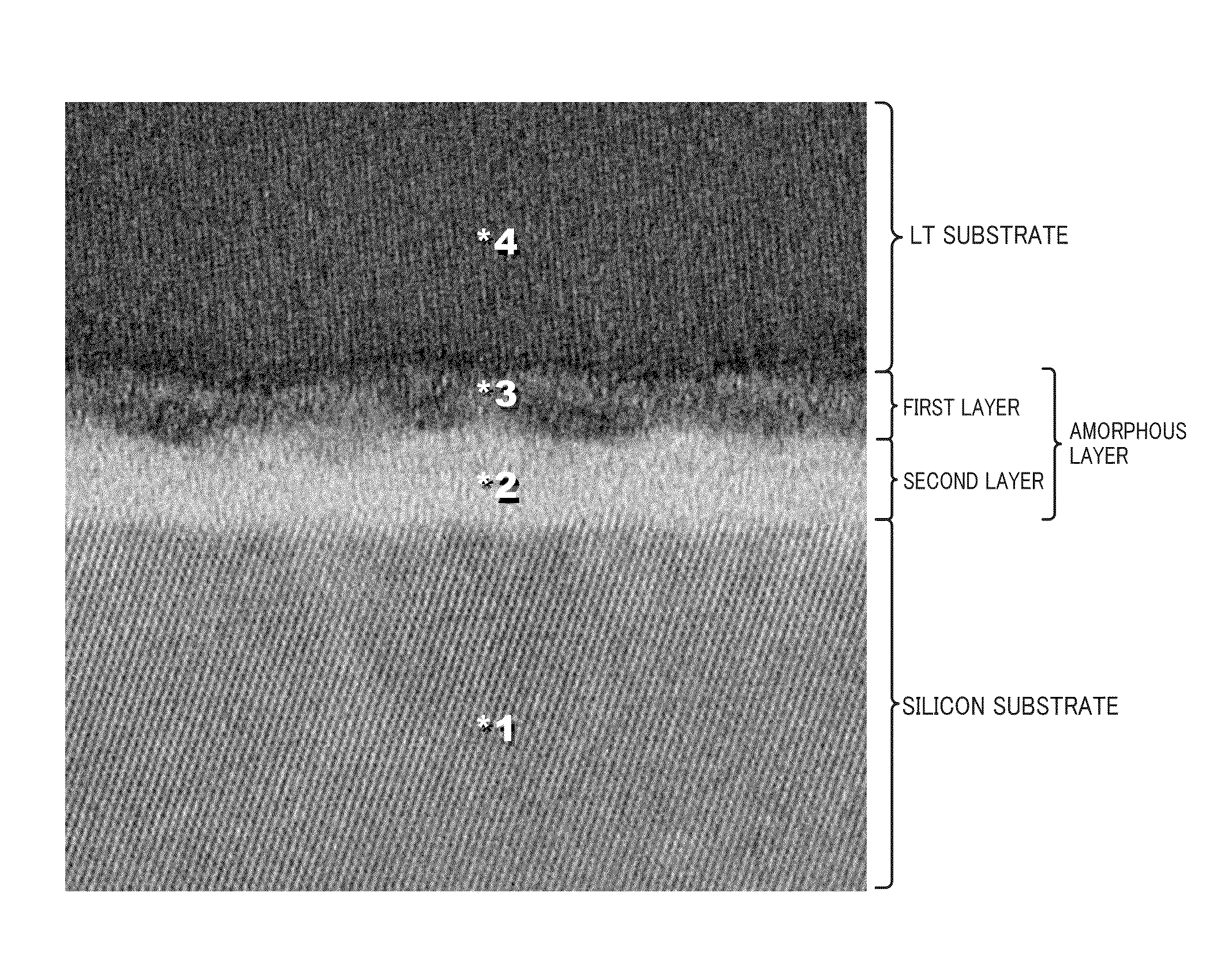
[0041]An LT substrate having a mirror finish on each side thereof and having a thickness of 230 μm and a silicon substrate having a mirror finish on each side thereof and having a thickness of 250 μm were prepared. The LT substrate used was a 42°-rotated Y-cut X-propagation LT substrate (42° Y-X LT), which is rotated by 42° from the Y axis toward the Z axis about the X axis, which is the direction in which a surface acoustic wave propagates. After the joining surface of each substrate was cleaned to remove soil therefrom, it was introduced into a vacuum chamber. The joining surface of each substrate was irradiated with a high-speed neutral argon atom beam (at an acceleration voltage of 1 kV and an argon flow rate of 60 sccm) in a vacuum on the order of 10−6 Pa for 70 seconds. After irradiation, each substrate was left standing for 10 minutes to cool the substrate to 26° C. to 28° C. The LT substrate and the silicon substrate were then joined together by bringing into contact the surfaces of the two substrates irradiated with the beam and pressing the two substrates together at 4.90 kN for 2 minutes. After joining, the LT substrate was polished to a thickness of 30 μm, and the two substrates were then annealed at 260° C. to obtain a composite substrate.
[0042]The composite substrate was cut to examine a cross-section under a transmission electron microscope (TEM). The results are shown in FIG. 1. As shown in FIG. 1, the amorphous layer had a thickness of 7 nm. The amorphous layer included, in order from the LT substrate toward the silicon substrate, a first layer, a second layer, and a third layer. The third layer was thicker than the first and second layers. The LT substrate, the first to third layers of the amorphous layer, and the silicon substrate were examined by composition analysis and elemental analysis using EDX. FIGS. 2 to 6 show the results of the composition analysis. In FIGS. 2 to 6, “point n” (where n is an integer of 1 to 5) denotes the position of “*n” in FIG. 1, which also applies to Table 1, described later. As can be seen from the results of the composition analysis, argon was detected in all of the first to third layers. The molybdenum peaks in FIGS. 2 to 6 are attributed to the sample holder. Table 1 shows the results of the elemental analysis. As can be seen from Table 1, the first layer contained 5 atomic percent of argon atoms, the second layer contained 9 atomic percent of argon atoms, and the third layer contained 3 atomic percent of argon atoms. No iron atoms were detected in any portion. The entire amorphous layer contained 8 atomic percent of argon atoms. A 2 mm square chip was cut from the composite substrate and was heated on a hot plate. After the chip was gradually heated from room temperature above 300° C., it was found to suffer no damage such as cracks or peeling. Because further heating was difficult on the hot plate, the chip was transferred to a rapid annealing furnace and was rapidly heated to 400° C. The chip was removed from the furnace and was found to suffer no damage.
TABLE 1 Element, By Unit of atm % Point Si Ar Ta Fe LT Substrate 5 35 0 65 0 Amorphous Layer First Layer 3 50 5 5 0 Second Layer 4 70 9 21 0 Third Layer 2 94 3 3 0 Si Substrate 1 100 0 0 0

Example

Example 2
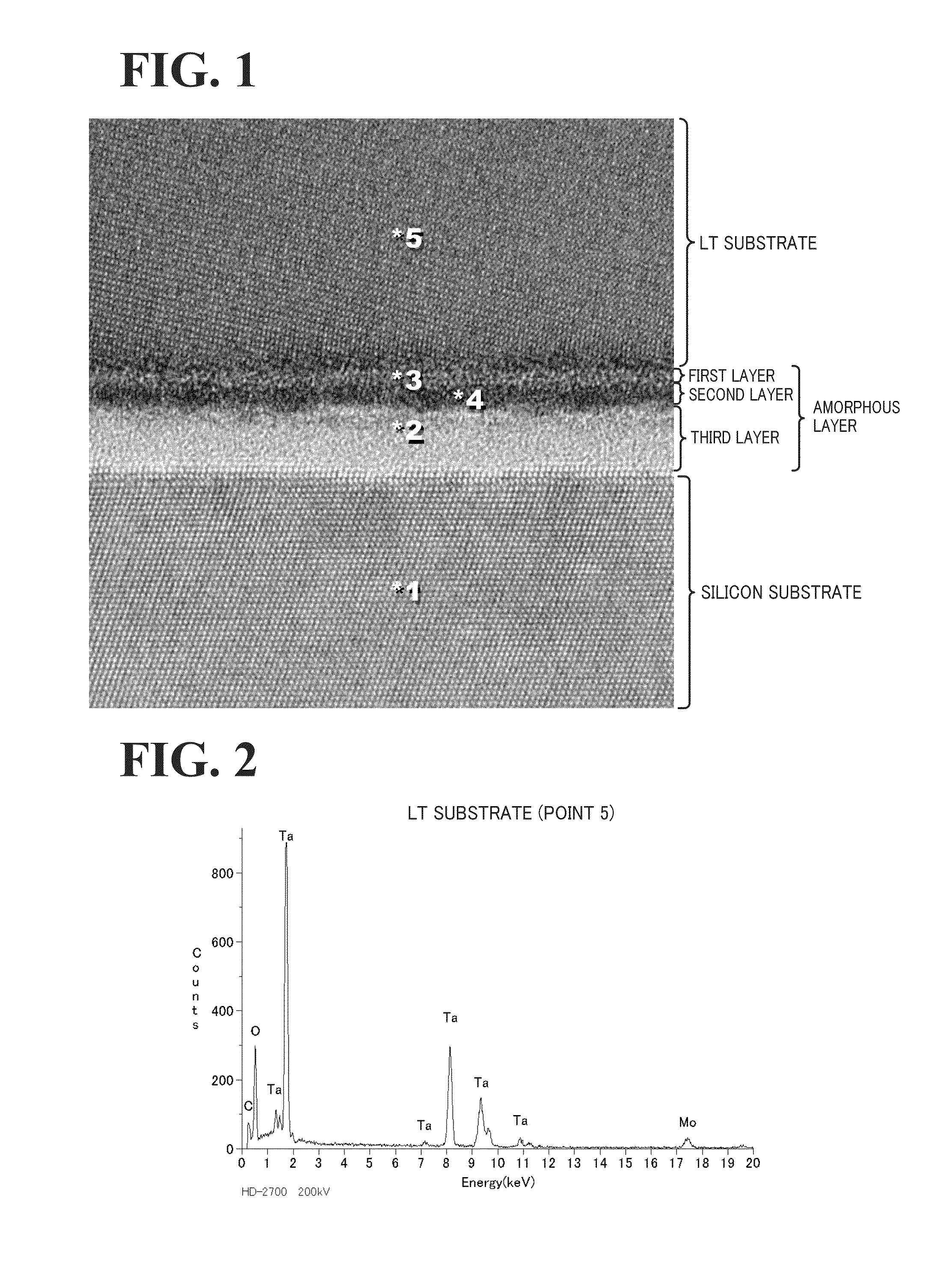
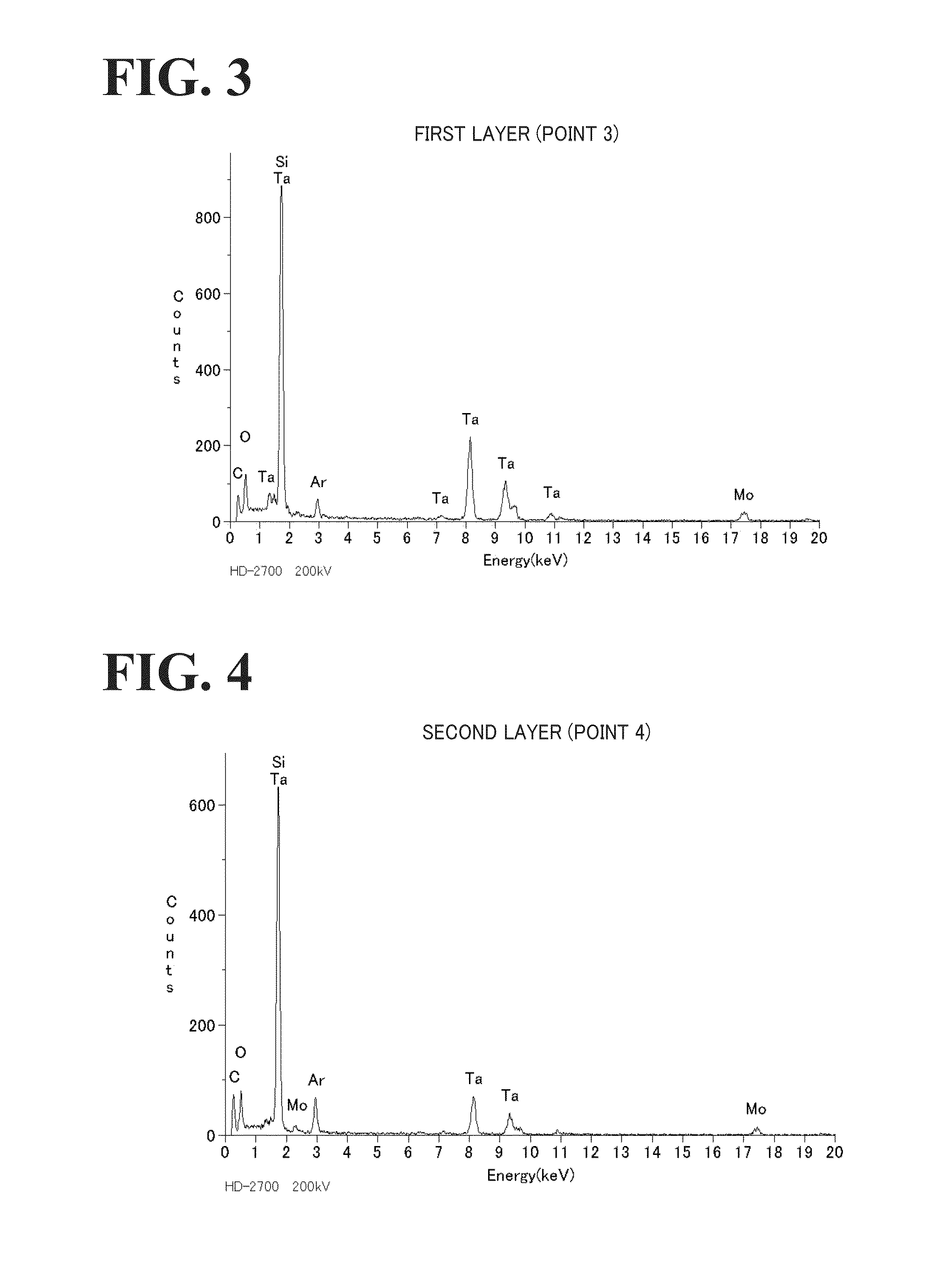
[0043]A composite substrate was manufactured as in Example 1 except that each substrate was irradiated with a high-speed neutral argon atom beam for 15 seconds, and a portion thereof was cut to examine a cross-section under a TEM. As a result, the amorphous layer had a thickness of about 2.5 nm. The amorphous layer included, in order from the LT substrate toward the silicon substrate, a first layer, a second layer, and a third layer. The third layer was thicker than the first and second layers. The LT substrate, the first to third layers of the amorphous layer, and the silicon substrate were examined by composition analysis and elemental analysis using EDX. According to the composition analysis, argon was detected in all of the first to third layers. According to the elemental analysis, the first layer contained 1 atomic percent of argon atoms, the second layer contained 3 atomic percent of argon atoms, and the third layer contained 0.4 atomic percent of argon atoms. No iron atoms were detected in any portion. The entire amorphous layer contained 2 atomic percent of argon atoms. The first layer contained a larger amount of a constituent element (tantalum) of the piezoelectric substrate than the second and third layers, and the third layer contained a larger amount of a constituent element (silicon) of the support substrate than the first and second layers. When a 2 mm square chip was gradually heated on a hot plate, as in Example 1, the LT substrate peeled off immediately above 300° C.

Example

Example 3
[0044]A composite substrate was manufactured as in Example 1 except that each substrate was irradiated with a high-speed neutral argon atom beam for 600 seconds, and a portion thereof was cut to examine a cross-section under a TEM. As a result, the amorphous layer had a thickness of about 15 nm. The amorphous layer included, in order from the LT substrate toward the silicon substrate, a first layer, a second layer, and a third layer. The third layer was thicker than the first and second layers. The LT substrate, the first to third layers of the amorphous layer, and the silicon substrate were examined by composition analysis and elemental analysis using EDX. According to the composition analysis, argon was detected in all of the first to third layers. According to the elemental analysis, the first layer contained 15 atomic percent of argon atoms, the second layer contained 21 atomic percent of argon atoms, and the third layer contained 13 atomic percent of argon atoms. No iron atoms were detected in any portion. The entire amorphous layer contained 18 atomic percent of argon atoms. The first layer contained a larger amount of a constituent element (tantalum) of the piezoelectric substrate than the second and third layers, and the third layer contained a larger amount of a constituent element (silicon) of the support substrate than the first and second layers. When a 2 mm square chip was heated on a hot plate, as in Example 1, the LT substrate peeled off immediately above 300° C.

PUM

no PUM

Description & Claims & Application Information

We can also present the details of the Description, Claims and Application information to help users get a comprehensive understanding of the technical details of the patent, such as background art, summary of invention, brief description of drawings, description of embodiments, and other original content. On the other hand, users can also determine the specific scope of protection of the technology through the list of claims; as well as understand the changes in the life cycle of the technology with the presentation of the patent timeline. Login to view more.

Similar technology patents

Thermal Shield at Casing Joint

InactiveUS20100074735A1Reduce thermal stressReduce amount of heat transferPump componentsReaction enginesGas turbinesProduct gas
Owner:SIEMENS ENERGY INC

Gas deep carburizing method for stainless steel

InactiveCN104099558ALower carburizing temperatureReduce thermal stressSolid state diffusion coatingTolueneCarburizing
Owner:GUIZHOU HONGLIN MACHINERY

Classification and recommendation of technical efficacy words

  • Improve adhesive strength
  • Reduce thermal stress

Capacitor and method of manufacturing the same

ActiveUS20170127521A1Improve adhesive strengthIncrease capacitance of capacitorFixed capacitor electrodesFinal product manufactureEngineeringCapacitor
Owner:SAMSUNG ELECTRO MECHANICS CO LTD

Lead frame

ActiveUS9653385B1Improve adhesive strengthSemiconductor/solid-state device detailsSolid-state devicesSilver oxideMoisture
Owner:SDI CORPORATION

Wafer processing base

ActiveUS20120202036A1Improve adhesive strengthImprove efficiencyFilm/foil adhesivesPolyureas/polyurethane adhesivesEngineeringResidual stress
Owner:LG CHEM LTD

Packaging substrate

Owner:PHOENIX PRECISION TECH CORP
Why Eureka
Try Eureka