Compound tunneling field effect transistor integrated on silicon substrate and method for fabricating the same

a tunneling field effect transistor and silicon substrate technology, applied in the direction of diodes, semiconductor devices, electrical devices, etc., can solve the problems of reducing the size of the smaller device, complicated process, and reaching the limi

Active Publication Date: 2014-10-02
THE BOARD OF TRUSTEES OF THE LELAND STANFORD JUNIOR UNIV +2
View PDF0 Cites 30 Cited by
  • Summary
  • Abstract
  • Description
  • Claims
  • Application Information

AI Technical Summary

Benefits of technology

[0031]To achieve the objective of the present invention, a compound tunneling field effect transistor according to the present invention has the first exemplary mode comprising: a silicon substrate; a source region formed of a first semiconductor material having a lattice constant difference with silicon 5% or less, a bandgap at least 0.4 electron volts (eV) narrower than that of silicon and a first conductive type on the silicon substrate; a channel region formed of a second semiconductor material having a lattice constant difference with the first semiconductor material 2% or less, a bandgap wider th...

Problems solved by technology

Thus, there is a problem that an optical integrated system must be fabricated through complicated processes.
Namely, the problem has occurred in the fabrication of the optical integrated system through the separation process for an optical device forming region and a peripheral circuit forming region.
However, it is reached to limit because of needs of a higher effective device and a smaller device with size decreased gradually by increasing integrity degree.
Namely, as mentioned in Korean Patent No. 10-1058370, the conventional MOSFET has a basic problem of a considerable decrease in performance in case of a low driving voltage due to the physical limit, i.e., a subthreshold swing (SS) of MOSFET cannot be lower than 60 mV/dec at room temperature.
However, a tunneling field effect transistor controls flows of electrons or holes by a tunneling mechanism which differs from a thermionic emission of the conventional MOSFET, and a finer change of input voltage (driving voltage) can bring on a larger change in output current.
However, because a driving current of a tunneling field effect transistor is induced by a tunneling phenomenon, current value lower than that of MOSFET is a problem.
Thus, a first technological problem to completely substitute a tunneling field effect transistor for a MOSFET is to be increasing a driving current (ION) to the value similar to that of a driving current of MOSFET.
It is considered as a problem for decreasing ON/OFF current ratio.
Specifically, it increases the consumption of a standby power in portable electronic devices.
And so a second technological problem to completely substitute for a MOSFET is urgently minimizing the OFF current.
And so there is a problem that it is difficult to control easily the threshold voltage by a boro...

Method used


Image

  • Compound tunneling field effect transistor integrated on silicon substrate and method for fabricating the same
  • Compound tunneling field effect transistor integrated on silicon substrate and method for fabricating the same
  • Compound tunneling field effect transistor integrated on silicon substrate and method for fabricating the same

Examples


embodiment 1

on a Device Structure

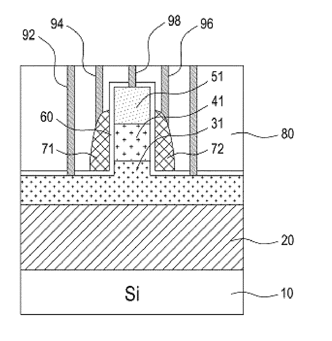
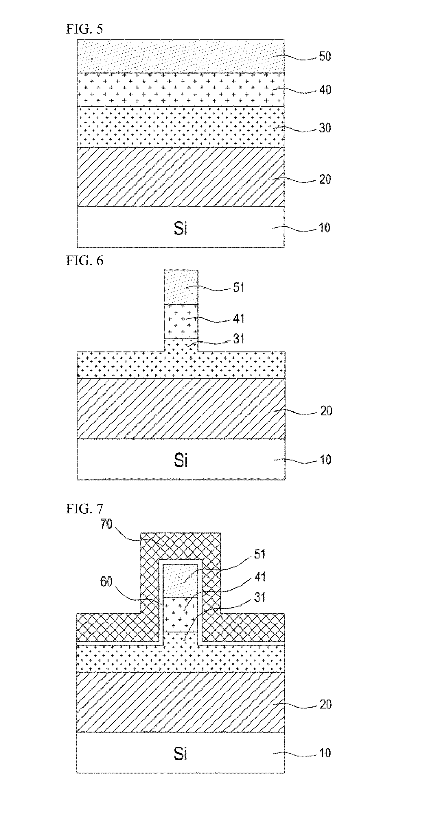
[0073]A compound tunneling field effect transistor according to Embodiment 1 of the present invention, as commonly shown in FIGS. 8 and 16, basically comprising: a silicon substrate 10; a source region 31 or 32 formed of a first semiconductor material having a lattice constant difference with silicon 5% or less, a bandgap at least 0.4 electron volts (eV) narrower than that of silicon and a first conductive type on the silicon substrate 10; a channel region 41 or 42 formed of a second semiconductor material having a lattice constant difference with the first semiconductor material 2% or less, a bandgap wider than that of the first semiconductor material and electron mobility at least 5 times higher than that of silicon on the source region 31 or 32; a drain region 51 or 52 formed of a third semiconductor material having a lattice constant difference with the second semiconductor material 1% or less, a bandgap wider than or equal to that of the second semiconducto...

embodiment 2

on a Device Structure

[0103]A compound tunneling field effect transistor according to Embodiment 2 of the present invention, as commonly shown in FIGS. 21, 27 and 33, basically comprising: a silicon substrate 10; a source region 33 or 34 formed of a first semiconductor material having a lattice constant difference with silicon 5% or less, a bandgap at least 0.4 electron volts (eV) narrower than that of silicon and a first conductive type on the silicon substrate 10; a channel region 43 or 45 formed of a second semiconductor material having a lattice constant difference with the first semiconductor material 2% or less, a bandgap wider than that of the first semiconductor material and electron mobility at least 5 times higher than that of silicon being contacted laterally to the source region 33 or 34; a drain region 53 or 55 formed of a third semiconductor material having a lattice constant difference with the second semiconductor material 1% or less, a bandgap wider than or equal to ...

embodiment 3

on a Device Structure

[0111]A compound tunneling field effect transistor according to Embodiment 3 of the present invention, as commonly shown in FIGS. 8, 16, 21 and 27, in the compound tunneling field effect transistor according to Embodiments 1 and 2, further comprises a buffer layer 20 formed of silicon germanium (SiGe) between the silicon substrate 10 and the source region 31, 32, 33 or 34. Wherein the first semiconductor material is germanium (Ge), and wherein the second and third semiconductor materials are gallium arsenide (GaAs).

[0112]By the above configuration, Embodiment 3 has the effects according to Embodiments 1 and 2 and additional effects as the following.

[0113]By the further formation of the buffer layer 20 with silicon germanium (SiGe) between the silicon substrate 10 and the source region 31, 32, 33 or 34, the source region 31, 32, 33 or 34 can be unformly formed of germanium (Ge) overcoming a lattice constant difference with the first semiconductor material (Ge) on...


PUM


Abstract

Compound tunneling field effect transistors integrated on a silicon substrate are provided with increased tunneling efficiency and an abrupt band slope by forming a source region with a material having a bandgap at least 0.4 electron volts (eV) narrower than that of silicon to increase a driving current (ON current) by forming a channel region with a material having almost no difference in lattice constant from a source region and having a high electron mobility at least 5 times higher than silicon. ON/OFF current ratio simultaneously is increased by forming a drain region with a material having a bandgap at least as wide as a channel region material to restrain OFF current. Tunneling field effect transistors having various threshold voltages according to circuit designs are formed easily by adding a specific material with an electron affinity less than a source region material when forming a channel region.

Description

BACKGROUND[0001]1. Field of the Invention[0002]The present invention relates to tunneling field effect transistors (TFETs), and more particularly to tunneling field effect transistors formed by compound semiconductors on a silicon substrate and methods for fabricating the same.[0003]2. Description of the Related Art[0004]These days, it is aiming for a goal that not only switch devices, but also various kinds of optical devices are integrated on a silicon substrate due to cost-effectiveness.[0005]So far, the optical devices in many cases are basically fabricated with direct bandgap compound semiconductors, but the various kinds of switch device of peripheral circuits for driving the optical devices are fabricated on a silicon substrate. Thus, there is a problem that an optical integrated system must be fabricated through complicated processes.[0006]Namely, the problem has occurred in the fabrication of the optical integrated system through the separation process for an optical device...

Claims


Application Information

Patent Timeline
IPC IPC(8): H01L29/775H01L29/66
CPCH01L29/66439H01L29/775H01L29/267H01L29/42312H01L29/66356H01L29/7391H01L29/0657
Inventor PARK, BYUNG-GOOKCHO, SEONGJAEKANG, IN MAN
Owner THE BOARD OF TRUSTEES OF THE LELAND STANFORD JUNIOR UNIV
Why Eureka
Try Eureka