

Power semiconductor device, method of manufacturing the device and bonding wire
- Summary
- Abstract
- Description
- Claims
- Application Information
AI Technical Summary
Benefits of technology
Problems solved by technology
Method used
Image

Examples
example 1
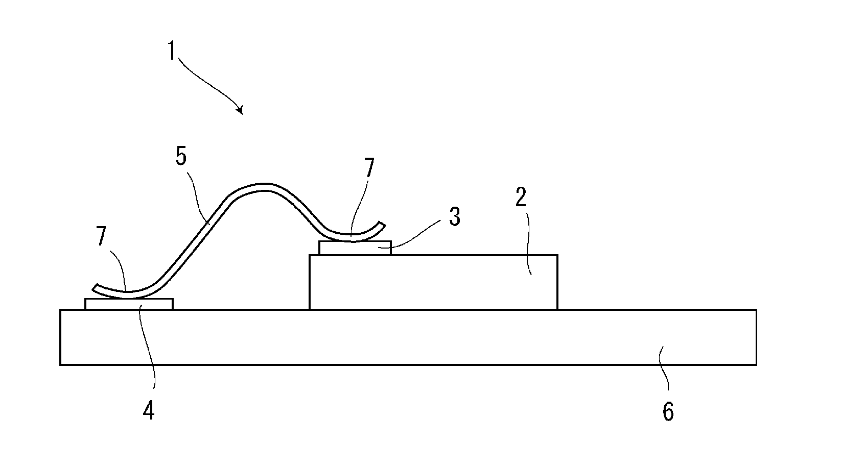
[0056]The power semiconductor shown in FIG. 1 is manufactured. A chip sample is made by forming a metal electrode with 2 μm thickness as a die electrode 3 on a 10 mm square semiconductor die 2. A substrate 6 is a 50 mm square Cu substrate with 4 μm Ag plating. Si or SiC die is used for the semiconductor die 2 and an Al electrode, Cu electrode, Ni electrode or Ti electrode is used as a metal electrode. Die bonding is made between the semiconductor die 2 and the substrate 6. Table 1 represents the manufacturing condition. In the examples of the present invention, one to four electrode coating layers listed in Table 1 are formed on the surface of the die electrode 3. No. 1 layer is the undermost layer on the electrode, No. 2-No. 4 layers are formed thereon as shown in Table 1. Types of metal of the coating layer and the thickness thereof are shown in Table 1.
[0057]Ag wire with 200 μm diameter is used as metal wire 5. Types of wire and RRR (residual resistance ratio of the wire) are sho...
example 2
[0063]A test is performed under a similar condition as example 1 except that the wire diameter is changed from 200 μmφ to 500 μmφ. The manufacturing condition and the result is shown in Table 2. Evaluation in example 2 is made in a similar way to example 1. In the case where the initial shear strength of 500 gf or more is attained, the evaluation of the initial shear strength is “good” represented by circles (symbol: ◯), and for other cases, the evaluation of the initial shear strength is “poor” represented by crosses (symbol: X). Same as example 1, any of examples of the invention shows good results.
TABLE 2Semi-Electrode coating layer(s)conductor Die No. 1 layerNo. 2 layerNo. 3 layerNo. 4 layerNodieelectrodetypethicknesstypethicknesstypethicknesstypethicknessExamples25SiAlZn 50 ÅNi5 μmAu200 Å—of the26SiAlNiV 500 ÅPd100 Å——Invention27SiAlTiW1000 ÅAu500 Å——WireStrengthBreakingInitialchangeelongationWire coating layershearafterChipNotypeRRR(%)typethicknessstrengthheatingdamageExamples...
PUM
 Abstract
Description
Claims
Application Information