Graphene-like nanosheet structure network on a substrate and the method for forming the same

a graphene-like nanosheet and structure network technology, applied in silicon compounds, oxy/sulfo carbides, carbides, etc., can solve the problems of reducing the graphene properties, unable to withstand high temperatures, and not being able to access ceramics, glass, metals and semi-conductor materials,

Active Publication Date: 2015-01-22
NANOMATERIAL INNOVATION
View PDF3 Cites 9 Cited by
  • Summary
  • Abstract
  • Description
  • Claims
  • Application Information

AI Technical Summary

Benefits of technology

[0016]The other objective of the invention is to provide a part or all of an article or a device comprising a surface having a nanostructure network bonding to the surface by a carbide bond, wherein Raman spectra of the nanostructure network have a G band at 1594±5 cm−1 and a D band at 1338±5 cm−1. Because Raman spectra of the nanostructure network is very similar to one of the graphene, the nanostructure is a graphene-like network. Furthermore, the nanosheet structure network has a carbide bond to the substrate.

Problems solved by technology

High-degree dispersion of graphenes in the polymer matrix can be realized, but it is not accessible for ceramics, glass, metals and semi-conductor materials because they are processed at temperatures above 400° C., at which graphenes are not thermally stable.
Since the graphene surface is very inert, individual graphene layers can be easily peeled off from a multi-layer stack and direct coating of graphene layers on the surface of solids requires the use of adhesives, w

Method used


Image

  • Graphene-like nanosheet structure network on a substrate and the method for forming the same
  • Graphene-like nanosheet structure network on a substrate and the method for forming the same
  • Graphene-like nanosheet structure network on a substrate and the method for forming the same

Examples


example 1

Silicon Carbide (and / or Silicon Oxycarbide) Bonded Graphene-Like Network Coated on Quartz Plates Using CVD of a Solid Carbon Source and a Silicone Source

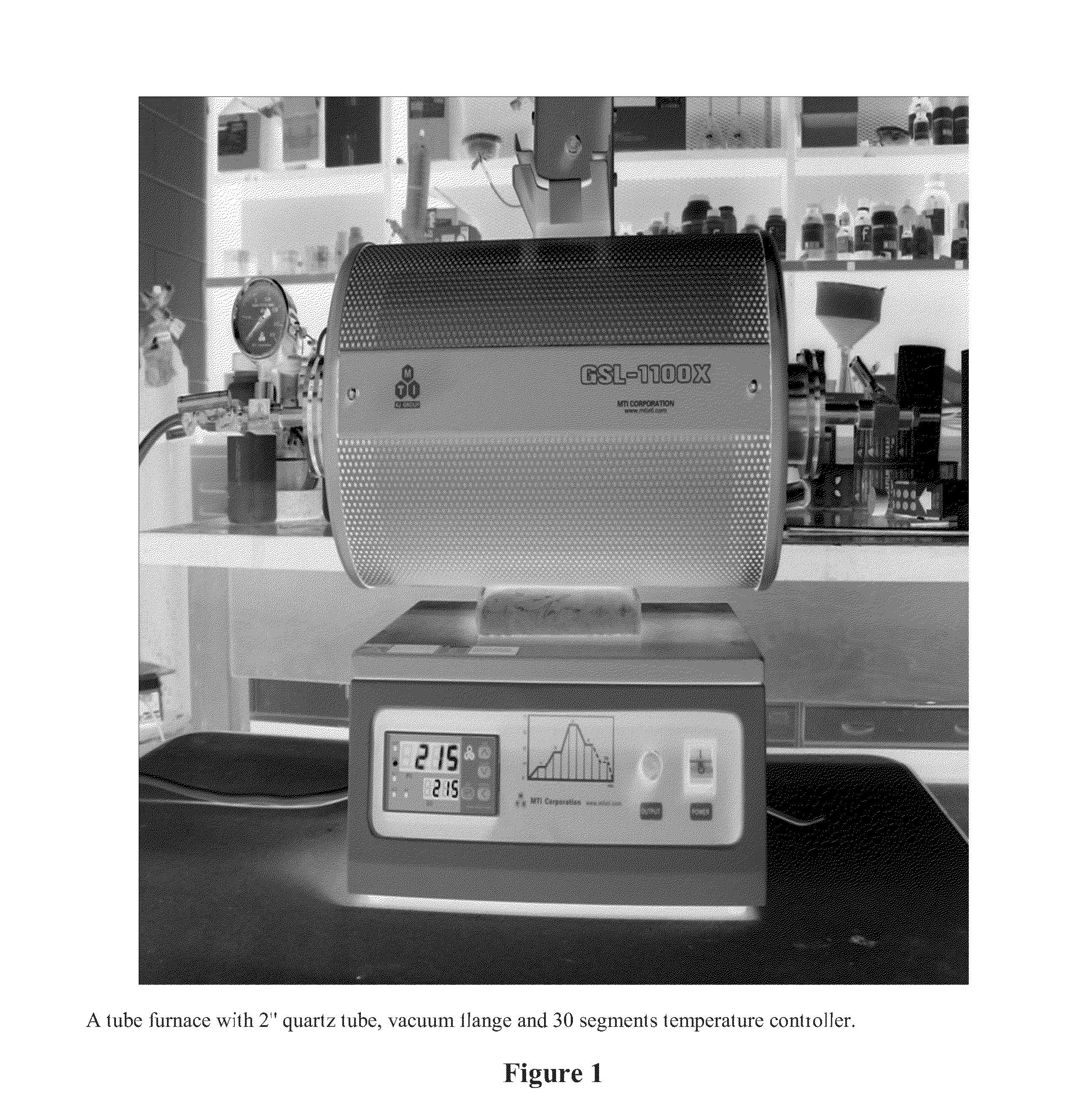
[0077]A solid carbon source, naphthalene (purchased from Aldrich, USA) with a purity of 99%, was used for the purpose of graphene formation and surface coating. Two 1 / 16″ thick quartz plates with 1″×1″ dimension and a piece of silicon-containing polymer or cyano-containing polymer with a weight of 1 gm were pre-placed inside the 2″ quartz tube of a furnaceinside the heating zone. 2 gm of naphthalene was also placed in the quartz tube, but outside the heating zone and near the gas inlet. An inert gas, Argon was applied to purge air inside the quartz tube with a flow rate of 300 SCCM for 10 minutes and then the flow rate was decreased to 200 SCCM. The temperature was quickly increased from room temperature to 750° C. under the inert gas atmosphere in the high temperature furnace and then the quartz tube outside the heating zone with t...

example 2

Silicon Carbide (and / or Silicon Oxycarbide) Bonded Graphene Network Coated on Silicon Wafers Using CVD of a Solid Carbon Source and a Silicon Source

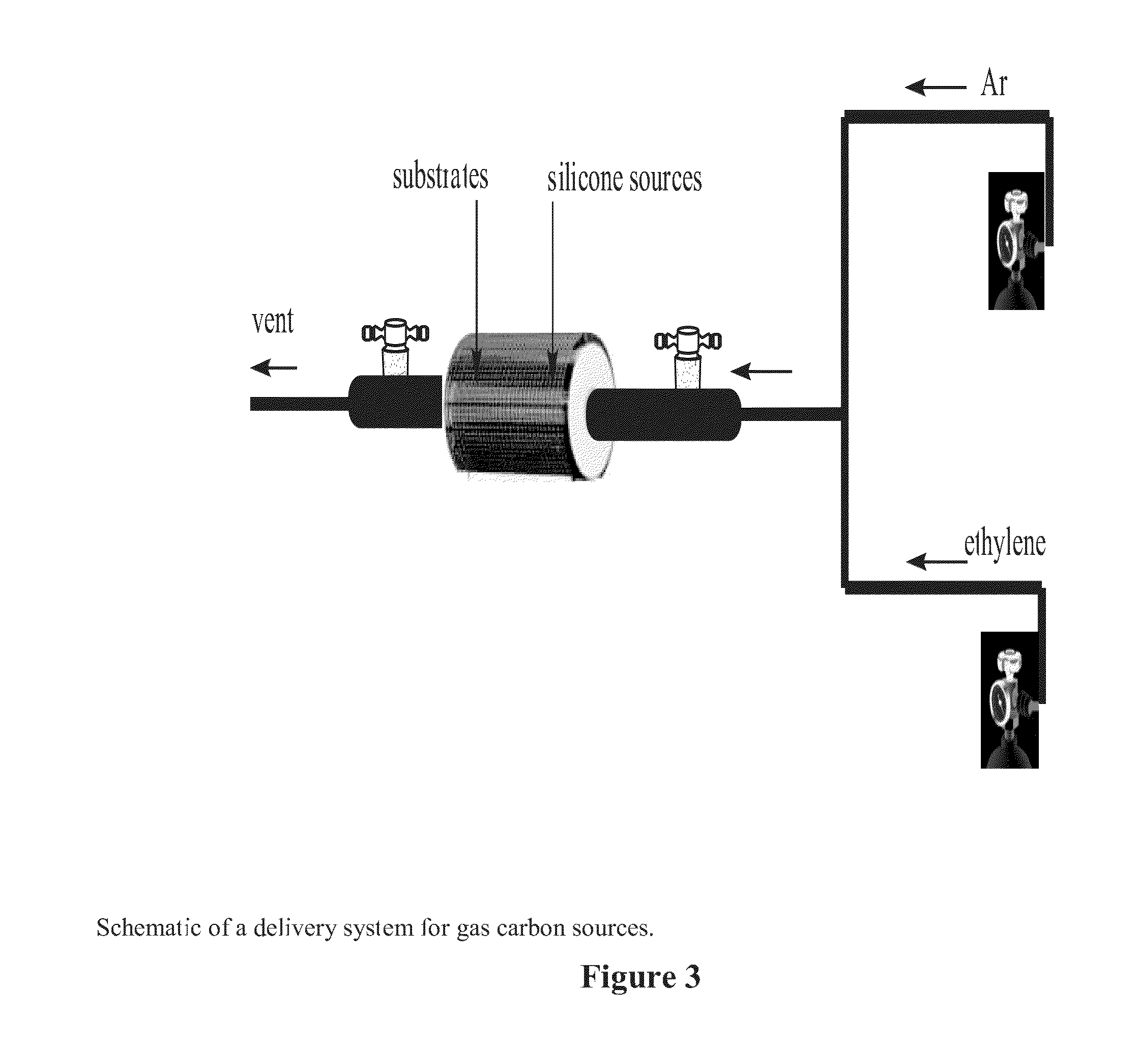
[0082]Similar to Example 1, two pieces of 2″ diameter silicon wafers and 1 grams of silicon-containing polymer were placed in the quartz tube inside the heating zone of the high temperature furnace. 2 grams of naphthalene were also placed outside the heating zone in the quartz tube with Ar gas atmosphere at a flow rate same as in Example 1. A similar thermal cycle was applied for coating and then the silicon wafers were from the quartz tube. FIG. 7 shows a Si wafer and a graphene-like network coated Si wafer.

example 3

Silicon Carbide (and / or Silicon Oxycarbide) Bonded Graphene-Like Network Coated on Quartz Plates Using CVD of Liquid Carbon Source and Liquid Silicon Source

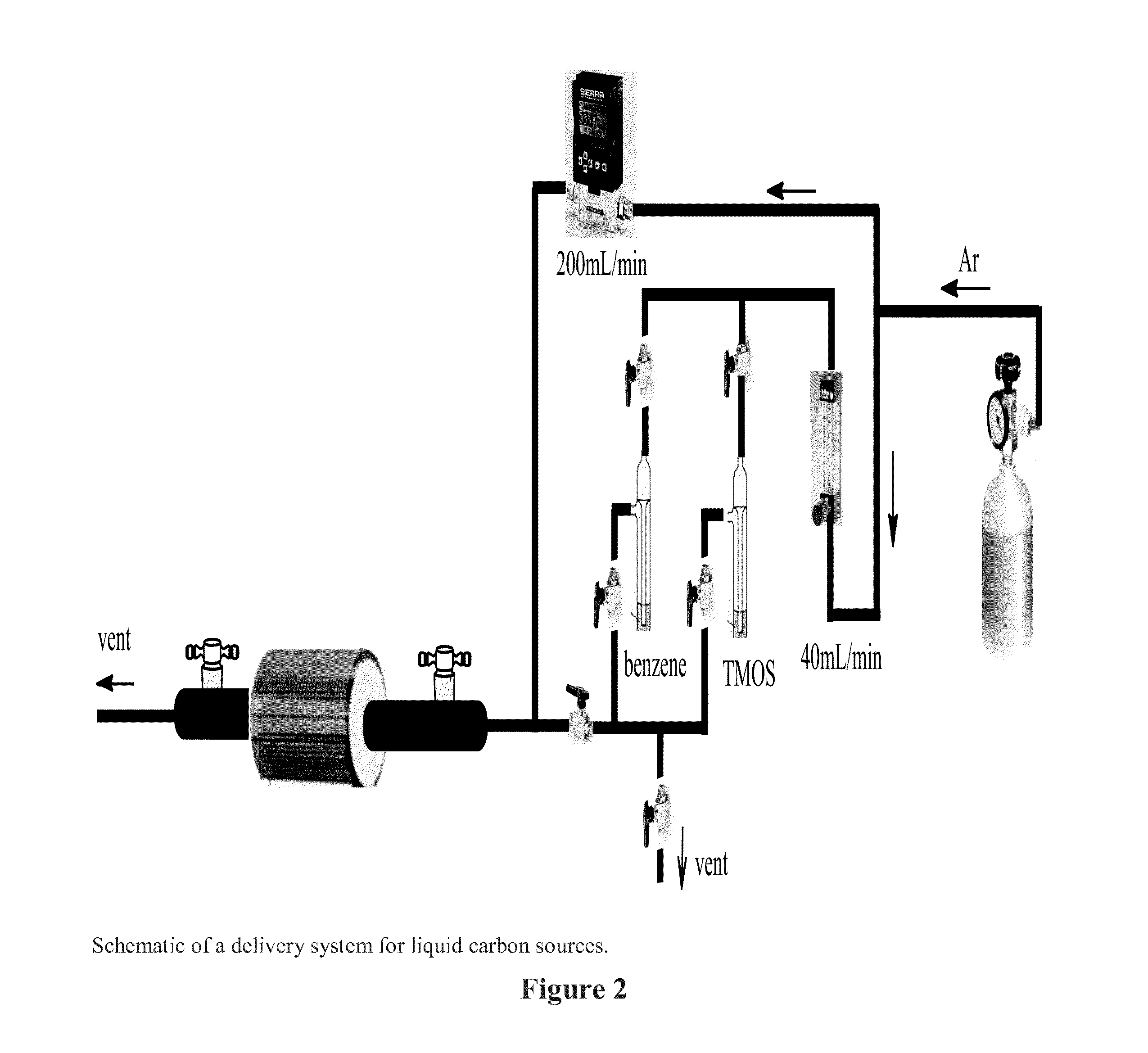
[0083]A liquid carbon source, benzene anhydrous (purchased from Aldrich, USA) with a purity of 99.8% in glass bubbler and a liquid silicon source, TMOS (Tetramethylorthosilicate, purchased from Aldrich, USA, 99.9%) in another glass bubbler were used for the purpose of graphene-like network and / or silicon carbide / oxycarbide bonded graphene-like network formation and surface coating. Two 1 / 16″ thick quartz plates with 1″×3″ dimension were pre-placed inside the 2″ quartz tube of a furnace inside the heating zone. An inert gas, Argon was applied to purge air inside the quartz tube with a flow rate of 300 SCCM for 10 minutes and then the flow rate was decreased to 200 SCCM. The temperature was increased from room temperature to 950° C. (at 20° C. / min) under the inert gas atmosphere. After the pre-specified temperature was reached, ben...


PUM

PropertyMeasurementUnit
Temperatureaaaaaaaaaa
Structureaaaaaaaaaa

Abstract

A facile method to produce covalently bonded graphene-like network coated on various solid substrates is disclosed in the present invention. According to one embodiment, a combination of chemical vapor deposition (CVD) of carbon sources and a silicon compound with or without a metal containing compound under an inert gas flow is processed at high temperatures to produce covalent carbide bonding among graphene-like structures and between graphene-like structures and substrate surface.

Description

TECHNICAL FIELD OF THE INVENTION[0001]The present invention relates to the network formation and coating of graphene-like nanosheets on the solid surfaces using chemical vapor deposition (CVD) of solid, gas, or liquid carbon sources together with a carbide source such as silicone rubber under an inert gas flow at elevated temperatures. Reactive carbon species from CVD form graphene-like structure and such structure is covalently bonded between each other and on the solid surface via carbide formation during the process. The solid surfaces include, but not limited to, ceramic, quartz, glass, silicon wafer, glass and quartz fibers, metals, metal alloys or the like. The presence of covalently-bonded graphene-like network coating on their surfaces makes non-conductive substrates thermally and electrically conductive and hydrophilic surfaces hydrophobic. It allows multiple graphene-like layers to be strongly bounded on solid surfaces by covalent bonds to achieve high temperature stabilit...

Claims


Application Information

Patent Timeline
IPC IPC(8): C01B31/04
CPCC01B31/0446C01B31/0453C01B31/301C01B31/36C23C16/0272C23C16/325C01B32/186C01B32/907C01B32/977
Inventor LEE, LYJAMESYU, JIANFENGYEN, YING-CHIEH
Owner NANOMATERIAL INNOVATION
Why Eureka
Try Eureka