Cooling plate, method for manufacturing the same, and member for semiconductor manufacturing apparatus

a semiconductor manufacturing and cooling plate technology, applied in the direction of manufacturing tools, soldering devices, lightening and heating devices, etc., can solve the problems of low heat dissipation ability of resins, easy decomposition, and easy deterioration, and achieve low cooling performance, easy manufacturing, and easy bonded together

Active Publication Date: 2015-03-19
NGK INSULATORS LTD
View PDF7 Cites 30 Cited by
  • Summary
  • Abstract
  • Description
  • Claims
  • Application Information

AI Technical Summary

Benefits of technology

[0017]In the cooling plate, the substrates bonded via the metal bonding layer are formed of the dense composite material. The dense composite material has a very small difference in linear thermal expansion coefficient from alumina and has sufficiently high thermal conductivity, denseness, and strength. Thus, a member for a semiconductor manufacturing apparatus manufactured by bonding such a cooling plate to an alumina ceramic member has a long life while maintaining high heat dissipation performance without separation between the cooling plate and the alumina ceramic member even when the member is repeatedly used between low temperatures and high temperatures. Substrates formed of the dense composite material are difficult to bond together by electron-beam welding. Substrates bonded together using a resin binder have low cooling performance. In the present invention, however, substrates can be relatively easily bonded together by thermal compression bonding (hereinafter abbreviated to TCB) using a metal bonding material and have high cooling performance.
[0018]In a cooling plate according to the present invention, preferably, the metal bonding layer contains as the metal bonding material an aluminum alloy bonding material containing Mg or Si and Mg and is formed by thermal compression bonding at a temperature lower than or equal to the solidus temperature of the bonding material. This results in higher cooling performance.
[0028]The cooling plate can be easily manufactured using the method for manufacturing a cooling plate. More specifically, substrates formed of the dense composite material are difficult to bond together by electron-beam welding. Substrates bonded together using a resin binder have low cooling performance. In the present invention, however, substrates can be relatively easily bonded together by thermal compression bonding using a metal bonding material and have high cooling performance.
[0029]In the step (c) of a method for manufacturing a cooling plate according to the present invention, preferably, the metal bonding material is an aluminum alloy bonding material containing Mg or Si and Mg, and thermal compression bonding is performed at a temperature lower than or equal to the solidus temperature of the bonding material. This results in a cooling plate having higher cooling performance.
[0034]The member for a semiconductor manufacturing apparatus has a long life while maintaining high heat dissipation performance without separation between the cooling plate and the alumina ceramic member even when the member is repeatedly used between low temperatures and high temperatures. The member for a semiconductor manufacturing apparatus can efficiently dissipate the heat from the electrostatic chuck to the cooling plate.

Problems solved by technology

However, since resins are organic materials, resins have low heat dissipation ability, decompose easily at high temperatures, and tend to deteriorate over time.
It is therefore difficult to use resins in a high temperature process for a long time.
However, unlike resins, metals are stiff and cannot relieve stress resulting from a difference in linear thermal expansion coefficient between an electrostatic chuck and a cooling plate.

Method used


Image

  • Cooling plate, method for manufacturing the same, and member for semiconductor manufacturing apparatus
  • Cooling plate, method for manufacturing the same, and member for semiconductor manufacturing apparatus
  • Cooling plate, method for manufacturing the same, and member for semiconductor manufacturing apparatus

Examples


first embodiment

Member for Semiconductor Manufacturing Apparatus—First Embodiment

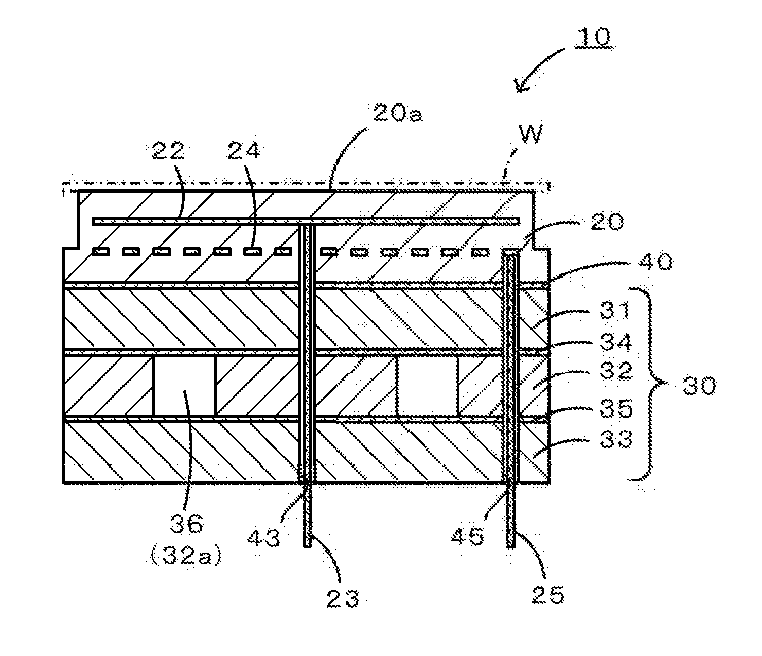
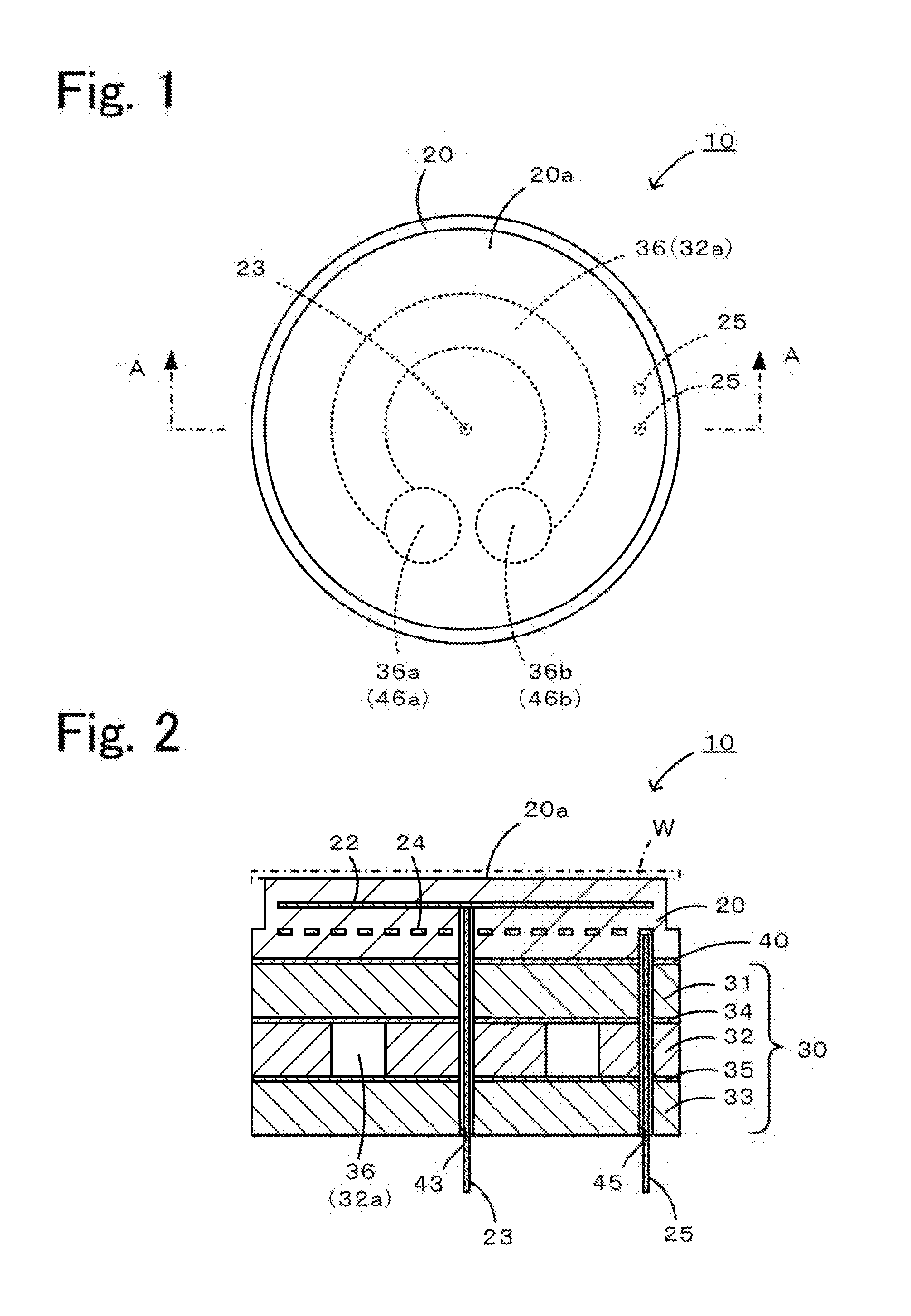
[0046]A member 10 for a semiconductor manufacturing apparatus according to a first embodiment will be described below. FIG. 1 is a plan view of the member 10 for a semiconductor manufacturing apparatus, and FIG. 2 is a cross-sectional view taken along the line A-A of FIG. 1.

[0047]The member 10 for a semiconductor manufacturing apparatus includes an alumina electrostatic chuck 20 for adsorbing a silicon wafer W to be subjected to plasma processing, a cooling plate 30 formed of a dense composite material having substantially the same linear thermal expansion coefficient as alumina, and a cooling plate-chuck bonding layer 40 for bonding between the electrostatic chuck 20 and the cooling plate 30.

[0048]The electrostatic chuck 20 is a disc-shaped alumina plate having an outer diameter smaller than the outer diameter of the wafer W and includes an electrostatic electrode 22 and a heater electrode 24. The electrostatic electr...

second embodiment

Member for Semiconductor Manufacturing Apparatus—Second Embodiment

[0058]A member 110 for a semiconductor manufacturing apparatus according to a second embodiment will be described below. FIG. 6 is a cross-sectional view of the member 110 for a semiconductor manufacturing apparatus.

[0059]The member 110 for a semiconductor manufacturing apparatus includes an alumina electrostatic chuck 20 for adsorbing a silicon wafer W to be subjected to plasma processing, a cooling plate 130 formed of a dense composite material having substantially the same linear thermal expansion coefficient as alumina, and a cooling plate-chuck bonding layer 40 for bonding between the cooling plate 130 and the electrostatic chuck 20.

[0060]The electrostatic chuck 20 is the same as in the first embodiment, has the same reference numerals as in the first embodiment, and will not be further described. The cooling plate 130 is a disc-shaped plate having an outer diameter slightly greater than or equal to the outer dia...

examples

Member for Semiconductor Manufacturing Apparatus

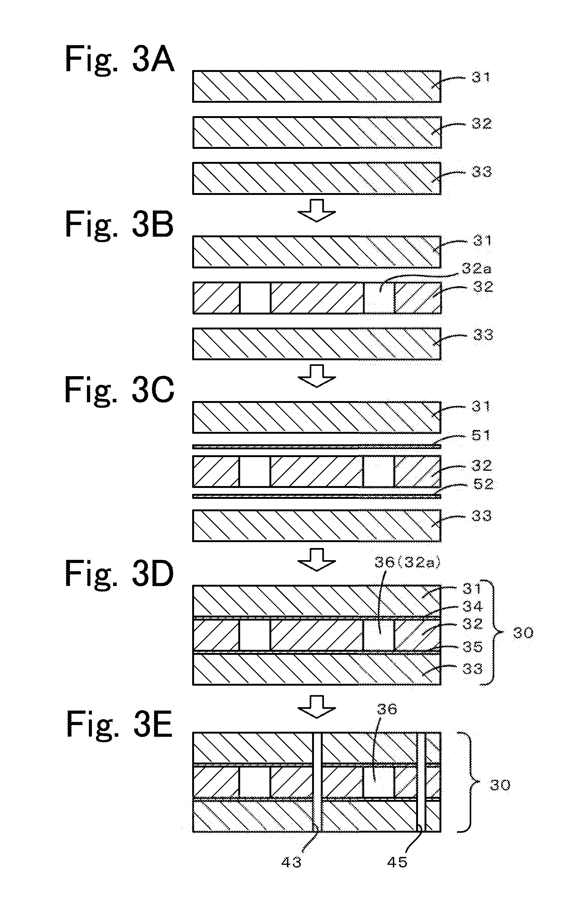
[0076]An electrostatic chuck 20 of a member 10 for a semiconductor manufacturing apparatus according to an example was made of alumina, was of Coulomb type, had a diameter of 297 mm, a thickness of 5 mm, and a dielectric film thickness (a thickness from an electrostatic electrode 22 to a wafer mounting face 20a) of 0.35 mm, and included a heater electrode 24 formed of a Nb coil. A cooling plate 30 was manufactured by TCB of first to third substrates 31 to 33 formed of a dense material described below in an experimental example 10 using an Al—Si—Mg bonding material (containing 88.5% by weight Al, 10% by weight Si, and 1.5% by weight Mg and having a solidus temperature of approximately 560° C.). In the TCB, the substrates were pressurized at a pressure of 1.5 kg / mm2 in a vacuum atmosphere at a temperature in the range of 540° C. to 560° C. for 5 hours. The cooling plate 30 had a diameter of 340 mm and a thickness of 32 mm. The electrosta...


PUM

PropertyMeasurementUnit
temperatureaaaaaaaaaa
bending strengthaaaaaaaaaa
lengthaaaaaaaaaa

Abstract

A member 10 for a semiconductor manufacturing apparatus includes an alumina electrostatic chuck 20, a cooling plate 30, and a cooling plate-chuck bonding layer 40. The cooling plate 30 includes first to third substrates 31 to 33, a first metal bonding layer 34 between the first and second substrates 31 and 32, a second metal bonding layer 35 between the second and third substrates 32 and 33, and a refrigerant path 36. The first to third substrates 31 to 33 are formed of a dense composite material containing Si, SiC, and Ti. The metal bonding layers 34 and 35 are formed by thermal compression bonding of the substrates 31 to 33 with an Al—Si—Mg or Al—Mg metal bonding material interposed between the first and second substrates 31 and 32 and between the second and third substrates 32 and 33.

Description

FIELD OF THE INVENTION[0001]The present invention relates to a cooling plate, a method for manufacturing the cooling plate, and a member for a semiconductor manufacturing apparatus.BACKGROUND OF THE INVENTION[0002]Electrostatic chucks are heated to high temperatures in a semiconductor process and have a cooling plate for heat dissipation. In this case, the material of the electrostatic chucks may be alumina, the material of the cooling plate may be aluminum, and a resin may be used as a bonding material. There is a very large difference in linear thermal expansion coefficient between alumina and aluminum. For example, alumina has a linear thermal expansion coefficient of 7.9 ppm / K (RT-800° C.: Uchida Rokakuho “Seramikku no butsuri (Physics of ceramics)”), and aluminum has a linear thermal expansion coefficient of 31.1 ppm / K (RT-800° C.: “Shinpen netsubussei handobukku (Thermophysical properties handbook new edition)”, edited by Japan Society of Thermophysical Properties). In such el...

Claims


Application Information

Patent Timeline
Patent Type & Authority Applications(United States)
IPC IPC(8): F28F3/12B23K1/19B23K1/00H01L21/683C04B35/56C04B35/58C04B37/00F28F21/08C04B35/565
CPCF28F3/12F28F21/086B23K1/19B23K1/0008H01L21/6833C04B35/5615C04B35/5611C04B35/58092C04B37/006C04B35/565C04B35/575H01L2221/683C04B35/645C04B2235/3839C04B2235/3843C04B2235/3891C04B2235/404C04B2235/428C04B2235/5436C04B2235/72C04B2235/77C04B2235/96C04B2235/9607Y10T428/249969
Inventor JINDO, ASUMIINOUE, KATSUHIROKATSUDA, YUJIKATAIGI, TAKASHIAMANO, SHINGOSUGIMOTO, HIROYA
Owner NGK INSULATORS LTD
Why Eureka
Try Eureka