Method for Manufacturing Germanide Interconnect Structures and Corresponding Interconnect Structures

a technology of interconnect structure and germanide, which is applied in the direction of solid-state devices, basic electric elements, electric devices, etc., can solve the problems that the known methods for obtaining the desired phase of metal germanides in dimensions below 30 nm are not suitable for interconnect fabrication of semiconductor devices, and achieve the effect of low resistivity

Active Publication Date: 2015-05-14
INTERUNIVERSITAIR MICRO ELECTRONICS CENT (IMEC VZW)
View PDF11 Cites 5 Cited by
  • Summary
  • Abstract
  • Description
  • Claims
  • Application Information

AI Technical Summary

Benefits of technology

[0005]It is an aim of the present disclosure to provide a method for forming interconn

Problems solved by technology

However, known methods for obtaining the desired phase of the metal germanides in dimensions below

Method used


Image

  • Method for Manufacturing Germanide Interconnect Structures and Corresponding Interconnect Structures
  • Method for Manufacturing Germanide Interconnect Structures and Corresponding Interconnect Structures
  • Method for Manufacturing Germanide Interconnect Structures and Corresponding Interconnect Structures

Examples


first embodiment

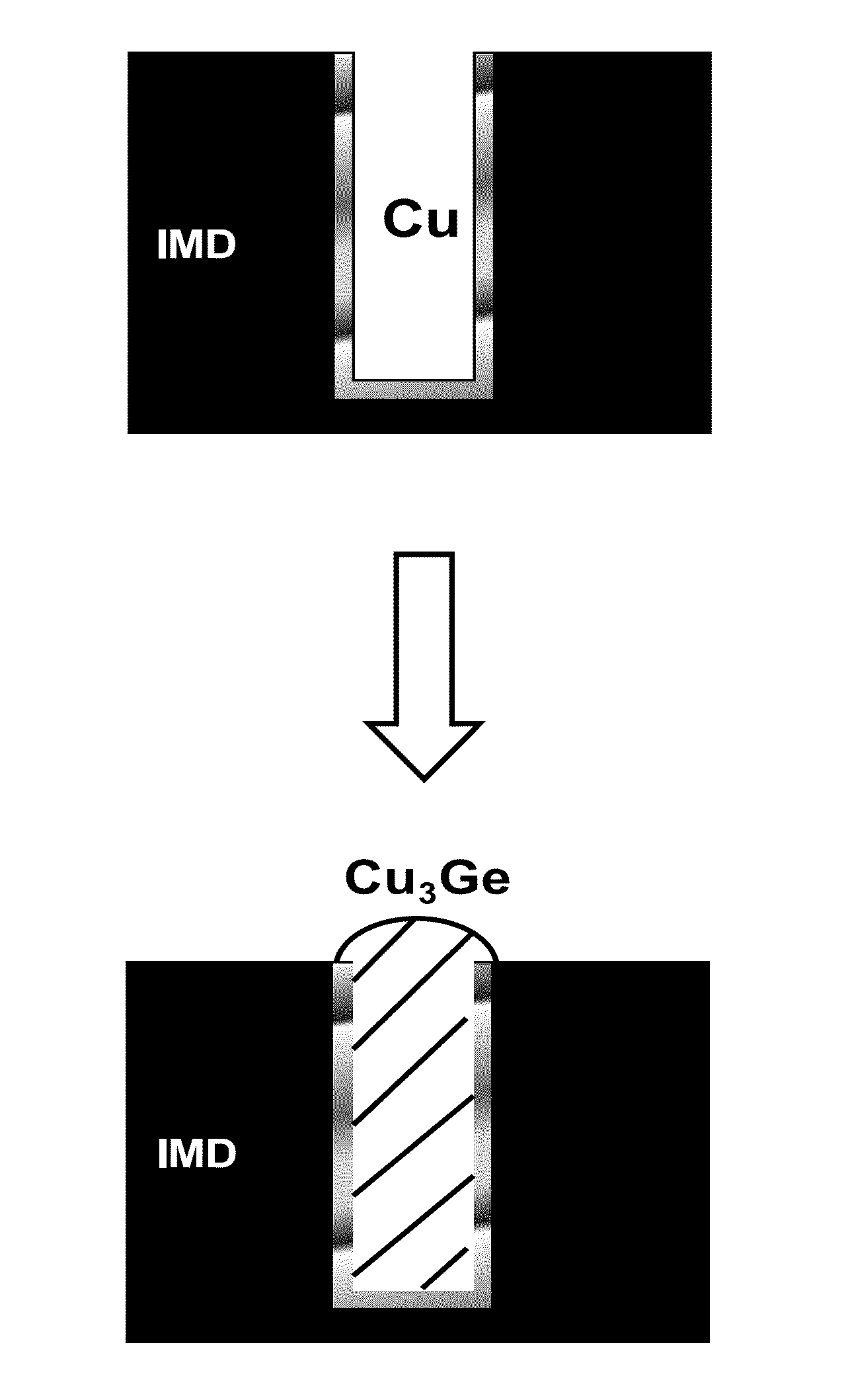
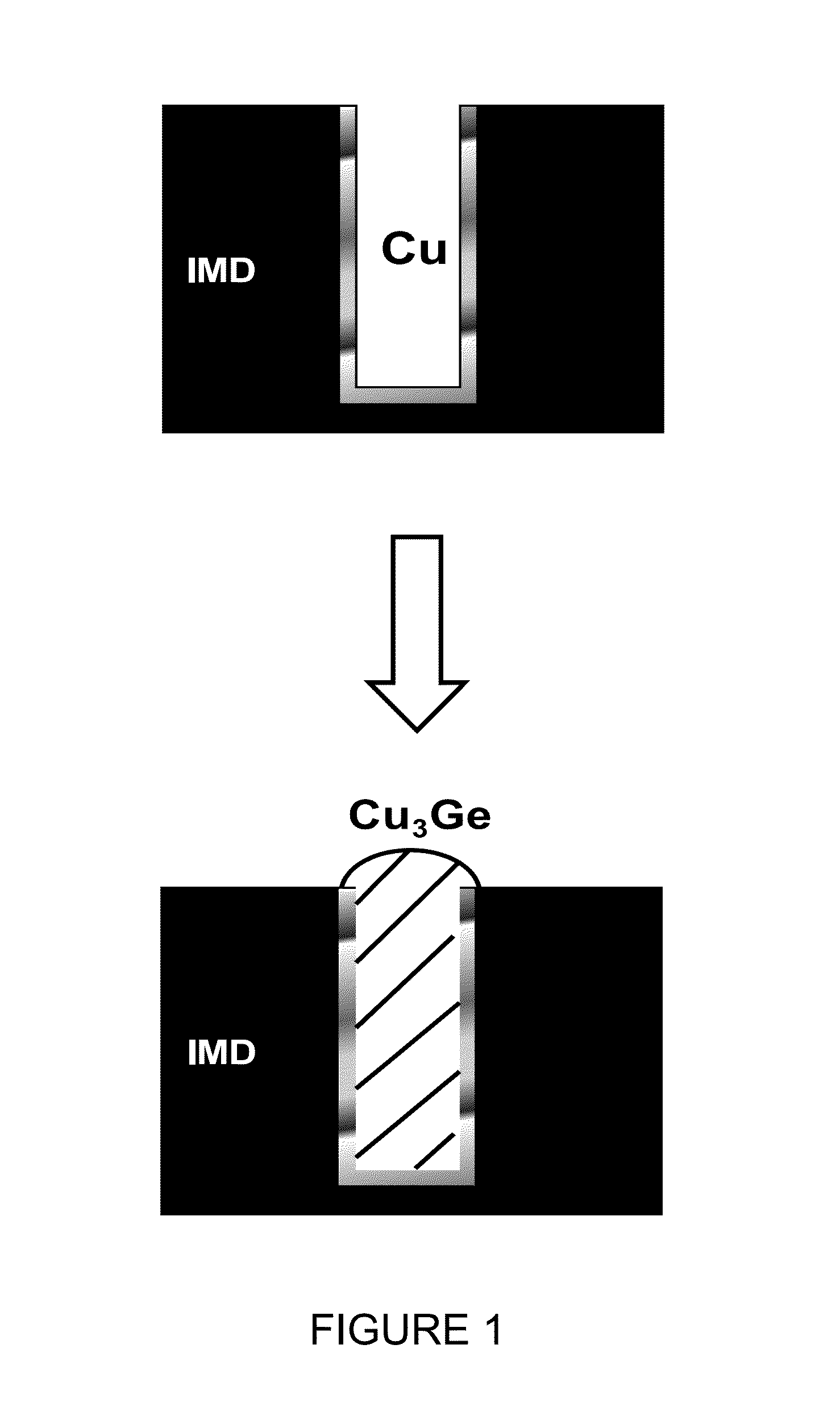
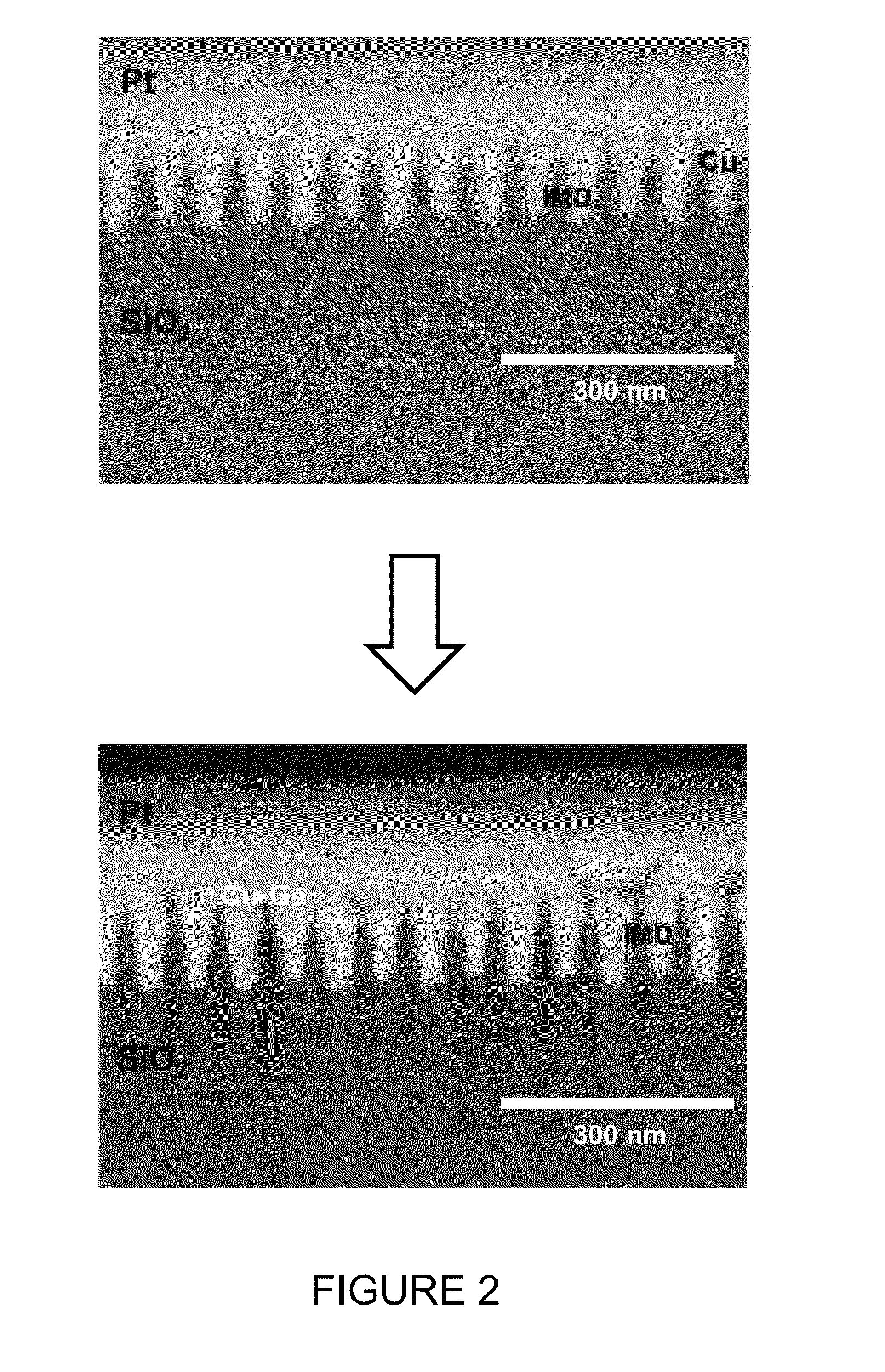
[0091]The method of the first embodiment allows a good phase control in both narrow and wide structures as compared to a solid state reaction approach.

[0092]Moreover the method of the first embodiment is applicable to Cu3Ge formation in all types of structures (e.g. vias, dual damascene) by adjusting the soak time to the thickness of the Cu which needs to be converted to Cu3Ge for a fixed soak temperature and partial pressure of the germanium precursor.

[0093]Advantageously, the method of the first embodiment is suitable for both on-pitch and large pitch structures. In general the on-pitch structures are structures for which the width and the spacing dimensions are available (i.e. 30 / 30 nm trenches), while the off-pitch structures are structures for which the width is different than the spacing (i.e. 30 / 140 nm trenches).

[0094]Preferably, an additional CMP can be introduced after the copper germanide formation to remove the Cu3Ge overgrowth and improve the electrical results for the o...

second embodiment

[0096] the present disclosure relates to a method for forming a nickel germanide (NiGe) alloy in interconnect structures. In preferred embodiments the disclosure relates to a method for forming a Nickel germanide (NiGe) alloy in narrow interconnect structures characterized by a half pitch of 10 nm or smaller.

[0097]As previously described, with the down scaling of the interconnects technology, in the sub-20 nm line width region, the resistivity of interconnects is expected to dramatically increase. To a large extent this can be attributed to the increased grain boundary and surface scattering caused by the low electron mean free path of Cu (39 nm). Therefore, a suitable replacement for copper (Cu) offering a low resistivity in the region of interest needs to be found.

[0098]Nickel germanide (NiGe) has been found to be a suitable replacement for Copper (Cu) in reducing the interconnect resistivity. Although, nickel germanide (NiGe) may exhibit higher bulk resistivity compared to Copper...

third embodiment

[0123] the present disclosure relates to a method for forming a cobalt germanide alloy (CoGe2) in interconnect structures. More specifically the present disclosure relates to a method for forming a cobalt germanide alloy (CoGe2) alloy in narrow interconnect structures characterized by a half pitch of 30 nm or smaller, preferably characterized by a half pitch of 10 nm or smaller.

[0124]Cobalt germanide alloy (CoGe2) has been found to be a suitable replacement to copper (Cu) in reducing the interconnect resistivity. Although the bulk resistivity of cobalt germanide alloy (CoGe2) alloy is higher compared to copper (Cu), the resistivity increase of cobalt germanide alloy (CoGe2) is slower for interconnect dimensions of 30 nm or smaller.

[0125]The present disclosure provides a method for obtaining a low resistivity cobalt germanide alloy (CoGe2) alloy in contacts and interconnects by using a solid vapor reaction between cobalt (Co) and germane precursor, such as GeH4, referred to herein as...


PUM


Abstract

Method for forming an interconnect structure, comprising the steps of: forming a recessed structure in a dielectric material on a substrate; at least partially filling said recessed structure with a metal chosen from the group consisting of copper, nickel and cobalt; introducing the substrate in a CVD reactor; bringing the substrate in the CVD reactor to a soak temperature and subsequently performing a soak treatment by supplying a germanium precursor gas to the CVD reactor at the soak temperature, thereby substantially completely converting the metal in the recessed structure to a germanide.

Description

TECHNICAL FIELD[0001]This disclosure relates to a method for manufacturing germanide interconnect structures and to the interconnect structures achievable by said method.BACKGROUND OF THE DISCLOSURE[0002]With the reduction of geometry sizes and the increase of aspect ratios, the ability to achieve a uniform Cu metallization becomes increasingly difficult. With the down scaling of the interconnect technology, in sub-30 nm line width regions, the resistivity of traditional copper (Cu) interconnects is expected to dramatically increase. This resistivity increase is mainly associated with the increased grain boundary and surface scattering of copper (Cu). Therefore, a copper (Cu) replacements needs to be found for the next generation of interconnects.[0003]Metal is a promising alternative as a potential replacement for Cu as interconnect metal due to the slow resistivity increase in dimensions below 30 nm. However, the suitability of metal is mainly determined by its filling ability and...

Claims


Application Information

Patent Timeline
IPC IPC(8): H01L23/528H01L21/321H01L23/532H01L21/768H01L21/02
CPCH01L23/528H01L21/76802H01L21/76879H01L21/3212H01L21/76843H01L23/53209H01L23/53238H01L21/02068H01L21/76883H01L23/53233H01L23/53261H01L21/76889H01L21/28518H01L21/76856H01L2924/0002H01L2924/00H01L21/76886
Inventor CARBONELL, LAURE ELISAPETER, ANTONY PREMKUMARSCHAEKERS, MARCVAN ELSHOCHT, SVENTOKEI, ZSOLT
Owner INTERUNIVERSITAIR MICRO ELECTRONICS CENT (IMEC VZW)
Why Eureka
Try Eureka