Devices, Structures, Materials and Methods for Vertical Light Emitting Transistors and Light Emitting Displays

a technology of light-emitting transistors and devices, applied in the direction of thermoelectric device junction materials, semiconductor devices, electrical apparatus, etc., can solve the problems of poor stability, unsuitable amoled pixels, and the lik

Active Publication Date: 2015-06-04
ATOM H2O LLC
View PDF5 Cites 38 Cited by
  • Summary
  • Abstract
  • Description
  • Claims
  • Application Information

AI Technical Summary

Benefits of technology

[0052]In still yet other embodiments, at least one of the drain, source, or gate electrodes comprise an electrode material selected from graphene sheets, doped Si, ZTO, ITO, Au, Al, Cu, Ni, Mo, Cr, Ag, metal nanowires, metal plate, metal meshes, metal grids, holey copper, holey graphene, conductive polymers, and a low coverage network of a plurality of nanowires.
[0053]In still yet other embodiments, the at least one conductive porous electrode is formed from a plurality of nanowires formed into one of the group of a random or patterned network of a plurality of metal or graphene nanowires, a nanowire metal mesh, a nanowire grid, and a nanowire network encased within an elastomeric material. In some such embodiments the plurality of nanowires are formed from a plurality of metal nanowires selected from Ag, Au and Cu having a diameter less than about 200 nm and a length greater than about 1 micron, and having a surface coverage less than 10%, a sheet resistance less than 100 Ω / sq and a transmission greater than 75%.

Problems solved by technology

However, the advances promised by AMOLEDs have not been realized at least partially as the result of limitations in conventional active matrix thin-film transistor (TFT) backplanes.
The current active matrix TFT backplanes used to drive AM-LCD pixels are typically made of amorphous silicon (a-Si), which has a low mobility (−1 cm2V−1s−1) and poor stability, and is therefore unsuitable for AMOLED pixels.
As a result of these deficiencies, currently AMOELD displays are driven by low temperature polycrystalline silicon (poly-Si) TFTs that suffer from high fabrication cost and time, and device size, orientation, and inhomogeneity limitations, all of which present a severe challenge to increasing display size and production yield.
However, in a conventional TFT architecture, the low-mobility of organic films requires a large source-drain voltage (>20 V) to turn on the OLED devices.
Though these approaches are promising, the required fabrication steps still limit the simplicity of system architecture and consequently production costs.

Method used


Image

  • Devices, Structures, Materials and Methods for Vertical Light Emitting Transistors and Light Emitting Displays
  • Devices, Structures, Materials and Methods for Vertical Light Emitting Transistors and Light Emitting Displays
  • Devices, Structures, Materials and Methods for Vertical Light Emitting Transistors and Light Emitting Displays

Examples


example 1

Spin Coating Ag NW Enabled VPLETs with Evaporated Dielectrics and Metal Gate Electrode on ITO

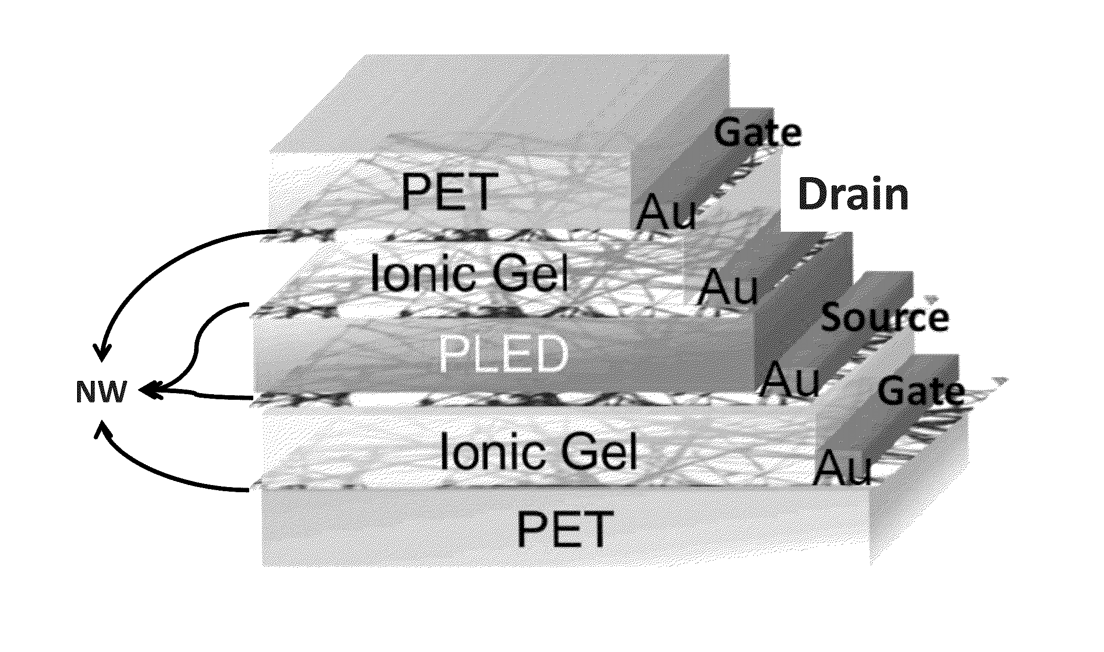
[0107]In one exemplary embodiment, shown schematically in FIG. 8, ITO was used as an anode and the transmission layer from which light from the light emitting cell may be emitted. A PEDOT / PSS (PH1000) was spin coated on the ITO at 2,000 rpm to serve as a drain electrode (D). After annealing at 140° C. for 10 minutes, super yellow THF solution was spin-coated at 5,000 rpm to form the PLED layer. On the top of super yellow layer (PLED), a 2 mg / mL Ag NW isopropanol solution was spin-coated at 2,000 rpm and reapplied for at least >5 times to form a conductive source electrode (S). Then a 200 nm thick silicon oxide was evaporated using low pressure chemical vapor deposition to form a dielectric layer. On top of the silicon oxide dielectric layer, 150 nm Al was sputter deposited using an electrode mask to form a gate electrode (G). The formed Ag NW enabled VPLETs were then characterized with a Kei...

example 2

Printing Ag NW Enabled VPLETs with ITO on Silicon Wafer

[0108]In one exemplary embodiment, printed Ag NW enabled VPLETs comprised of ITO as transparent porous conductive electrodes and light emitting polymers as channel materials on silicon wafer are provided. This process includes printing a uniform Ag NW network on silicon wafer, LEPs, and laminating PEDOT / PSS coated ITO with printed LEPs to achieve printed Ag NW enabled VPLETs with gate modulated brightness and external efficiency higher than PLEDs. Using aerosol jet printing technologies it is possible to print Ag NW networks on any substrate layer-by-layer allowing for the printing of a Ag NW enabled VPLET on silicon wafers of various SiO2 thickness.

[0109]LEPs (blue: PFO, green: super-yellow, red: MEH-PPV) have been fabricated into typical OLETs using thermal evaporated gold electrodes (70 nm thickness) with 20 μm channel length and 1000 μm channel width, and show a maximum power conversion efficiency of 0.002-0.005 Cd / A, an ext...

example 3

Printing Ag NW Enabled VPLETs with Ag NW Electrode on Si Wafer

[0111]In another embodiment, an aerosol jet printing technique is provided for printing Ag NW on flexible plastics such as polyethylene terephthalate (PET) to fabricate flexible transparent porous conductive electrodes. Printing uniform Ag NW on PET allows one to replace ITO. In a particular embodiment, printed Ag NW porous conductive electrodes will be spin-coated with PEDOT / PSS and then will be laminated with printed LEPs on Ag NW covered silicon wafer to achieve Ag NW enabled VPLETs with a Ag NW electrode on silicon wafer. Alternatively, it is possible to use the Ag NW stretchable electrode fabrication method described above. In one such method Ag NW is printed on the top of a substrate such as glass, and then in-situ polymerization is performed atop the Ag NW networks. The peeled-off polymer films are porous, transparent and conductive with the embedded Ag NWs.

[0112]As shown in FIGS. 10a and 10b, in this embodiment Ag...


PUM


Abstract

Devices, structures, materials and methods for vertical light emitting transistors (VLETs) and light emitting displays (LEDs) are provided. In particular, architectures for vertical polymer light emitting transistors (VPLETs) for active matrix organic light emitting displays (AMOLEDs) and AMOLEDs incorporating such VPLETs are described. Porous conductive transparent electrodes (such as from nanowires (NW)) alone or in combination with conjugated light emitting polymers (LEPs) and dielectric materials are utilized in forming organic light emitting transistors (OLETs). Combinations of thin films of ionic gels, LEDs, porous conductive electrodes and relevant substrates and gates are utilized to construct LETs, including singly and doubly gated VPLETs. In addition, printing processes are utilized to deposit layers of one or more of porous conductive electrodes, LEDs, and dielectric materials on various substrates to construct LETs, including singly and doubly gated VPLETs.

Description

RELATED APPLICATIONS[0001]This application claims priority to U.S. Provisional Application No. 61 / 907,324 filed Nov. 21, 2013, the disclosure of which is incorporated herein by reference.FIELD OF THE INVENTION[0002]Devices, structures, materials and methods for vertical light emitting transistors and light emitting displays are presented.BACKGROUND OF THE INVENTION[0003]Active Matrix Organic Light Emitting Diode (AMOLED) displays have been highly anticipated by electronic consumers due to their well-recognized advantages in power consumption, pixel brightness, viewing angle, response time, and contrast ratio over liquid crystal displays (LCD). (See, e.g., G. Gu and S. R. Forrest, IEEE Journal of Selected Topics in Quantum Electronics, vol. 4, pp. 83-99, 1998, the disclosure of which is incorporated herein by reference.) However, the advances promised by AMOLEDs have not been realized at least partially as the result of limitations in conventional active matrix thin-film transistor (...

Claims


Application Information

Patent Timeline
Patent Type & Authority Applications(United States)
IPC IPC(8): H01L33/00H01L33/32H01L51/56H01L33/34H01L51/52H01L33/06H01L33/30
CPCH01L33/0041H01L33/06H01L33/32H01L33/30H01L51/56H01L51/5296H01L33/0075H01L33/0062H01L33/0054H01L33/34H01L33/08H10K59/12H10K10/491H10K50/30H10K50/84H10K50/805H10K59/00H10K71/00H10K71/12H10K71/13H10K71/60H10K85/111H10K85/113H10K85/114H10K85/141H10K85/151H10K85/1135H10K2102/00H10K2102/103H01L27/15H01L33/0095H01L33/24H01L33/28H01L33/40H01L33/52H01L2933/0016H01L2933/005
Inventor LI, HUAPING
Owner ATOM H2O LLC
Why Eureka
Try Eureka