

TFT ion sensor and TFT ion sensor apparatus using the same
a technology of ion sensor and ion sensor, which is applied in the direction of instruments, semiconductor devices, measurement devices, etc., can solve the problems of inability to increase the sensitivity, difficult to detect a small amount of concentration substance such as hormone with high precision, and difficult to perform precise detection
- Summary
- Abstract
- Description
- Claims
- Application Information
AI Technical Summary
Benefits of technology
Problems solved by technology
Method used
Image

Examples
first exemplary embodiment
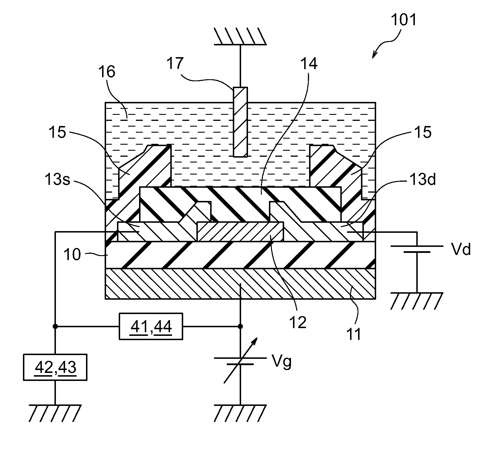
[0044]FIG. 1 is a sectional view showing a TFT ion sensor 101 according to a first exemplary embodiment.
[0045]The TFT ion sensor 101 includes: a semiconductor active layer 12 in which a source electrode 13s and a drain electrode 13d are connected; a thermal oxide film 10 as a gate insulating film and a silicon substrate 11 as a gate electrode provided on one of the surfaces of the semiconductor active layer 12; an ion sensitive insulating film 14 provided on the other surface of the semiconductor active layer 12; and a reference electrode 17 provided at a position spatially isolated from the ion sensitive insulating film 14, in which the electrostatic capacitance per unit area of the ion sensitive insulating film 14 is larger than the electrostatic capacitance per unit area of the gate insulating film (the thermal oxide film 10). Further, the TFT ion sensor 101 further includes either a voltage detection unit 41 which reads out the potential difference between the source electrode 1...
example 1
[0052]Next, Example 1 which is a more concrete form of the first exemplary embodiment will be described by referring to FIG. 1.
[0053]First, the silicon substrate 11 on which the thermal oxide film 10 having a thickness of 200 nm was prepared. Instead of the thermal oxide film 10, a silicon oxide film, a silicon nitride film, or the like deposited by a plasma CVD (Chemical Vapor Deposition) method or a sputtering method may also be used.
[0054]Further, an oxide semiconductor film having a thickness of 50 nm constituted with In—Ga—Zn—O was deposited by the sputtering method by using a metal mask on the silicon substrate 11 on which the thermal oxide film 10 was formed. At that time, a sinter target constituted with In—Ga—Zn—O was used, the substrate was not heated, and a DC (Direct Current) sputtering method was employed in a mixed gas atmosphere of an argon gas and an oxygen gas. After the deposition, annealing was performed at 400° C. for an hour. Through patterning the oxide semicon...
second exemplary embodiment
[0070]FIG. 3 is a sectional view showing a TFT ion sensor 102 according to a second exemplary embodiment.
[0071]A gate electrode 19 is formed on a glass substrate 18, and a gate insulating film 20 is formed further. An island shaped semiconductor active layer 12 is formed on the gate insulating film 20, and a source electrode 13s and a drain electrode 13d are formed to be in contact with a part of the top surface of the semiconductor active layer 12. An ion sensitive insulating film 14 is formed on the semiconductor active layer 12, the source electrode 13s, and the drain electrode 13d. Only the ion sensitive insulating film 14 in a region corresponding to the channel part of the semiconductor active layer 12 is exposed, and the other region is covered by a protection insulating film 15. The TFT of such structure is disposed within the sensing-target substance 16, and a reference electrode 17 is provided in the sensing-target substance 16.
[0072]It is the point of the second exemplary...
PUM
 Abstract
Description
Claims
Application Information