Composite Substrate, Elastic Wave Device, and Method for Producing Elastic Wave Device

a technology of elastic wave and composite substrate, which is applied in the direction of generator/motor, transportation and packaging, other domestic articles, etc., can solve the problems of low commercial value, increase in the cost of elastic wave device, and high cost of polishing, so as to reduce warpage of composite substrate in response to temperature changes, increase the strength of composite substrate, and increase the thickness

Active Publication Date: 2015-11-19
NGK INSULATORS LTD
View PDF0 Cites 19 Cited by
  • Summary
  • Abstract
  • Description
  • Claims
  • Application Information

AI Technical Summary

Benefits of technology

[0010]The present invention has been accomplished in order to overcome the problems. A main object is to achieve reduction in warpage of a composite substrate and enhancement of strength of the composite substrate and to suppress the corresponding increase in the production cost of elastic wave devices.
[0021]In a composite substrate according to the present invention, a support substrate is formed by directly bonding together a first substrate and a second substrate at a strength that allows separation with a blade, the first and second substrates being formed of the same material. Accordingly, the support substrate has a large thickness, compared with a case where the first substrate alone is used as the support substrate. As a result, warpage of the composite substrate in response to changes in temperature can be reduced and the strength of the composite substrate can also be increased. After elastic wave devices are formed, the thickness of the support substrate can be easily decreased by removing the second substrate from the first substrate by separation with a blade. This is thus achieved at a low cost, compared with a case where a thick support substrate is thinned by polishing. As a result, the corresponding increase in the production cost of elastic wave devices can be suppressed. The second substrate having been removed can be recycled for producing another composite substrate according to the present invention, which also contributes to cost reduction.
[0022]In a method for producing an elastic wave device according to the present invention, the above-described composite substrate according to the present invention is prepared; electrodes for elastic wave devices are formed on a surface of the piezoelectric substrate of the composite substrate; the second substrate is removed from the first substrate by separation with a blade; and dicing is subsequently carried out to obtain elastic wave devices. After electrodes for elastic wave devices are formed, the thickness of the support substrate can be easily decreased by removing the second substrate from the first substrate by separation with a blade. This is thus achieved at a low cost, compared with a case where a thick support substrate is thinned by polishing. As a result, the corresponding increase in the production cost of elastic wave devices can be suppressed.

Problems solved by technology

However, elastic wave devices produced from this composite substrate have an excessively large thickness, which is against the trend toward reduction in thickness and results in a low commercial value.
However, the polishing incurs a high cost, which results in an increase in the cost of elastic wave devices.
Accordingly, the cost of the elastic wave devices produced from the composite substrate increases, which is problematic.

Method used


Image

  • Composite Substrate, Elastic Wave Device, and Method for Producing Elastic Wave Device
  • Composite Substrate, Elastic Wave Device, and Method for Producing Elastic Wave Device
  • Composite Substrate, Elastic Wave Device, and Method for Producing Elastic Wave Device

Examples


example 1

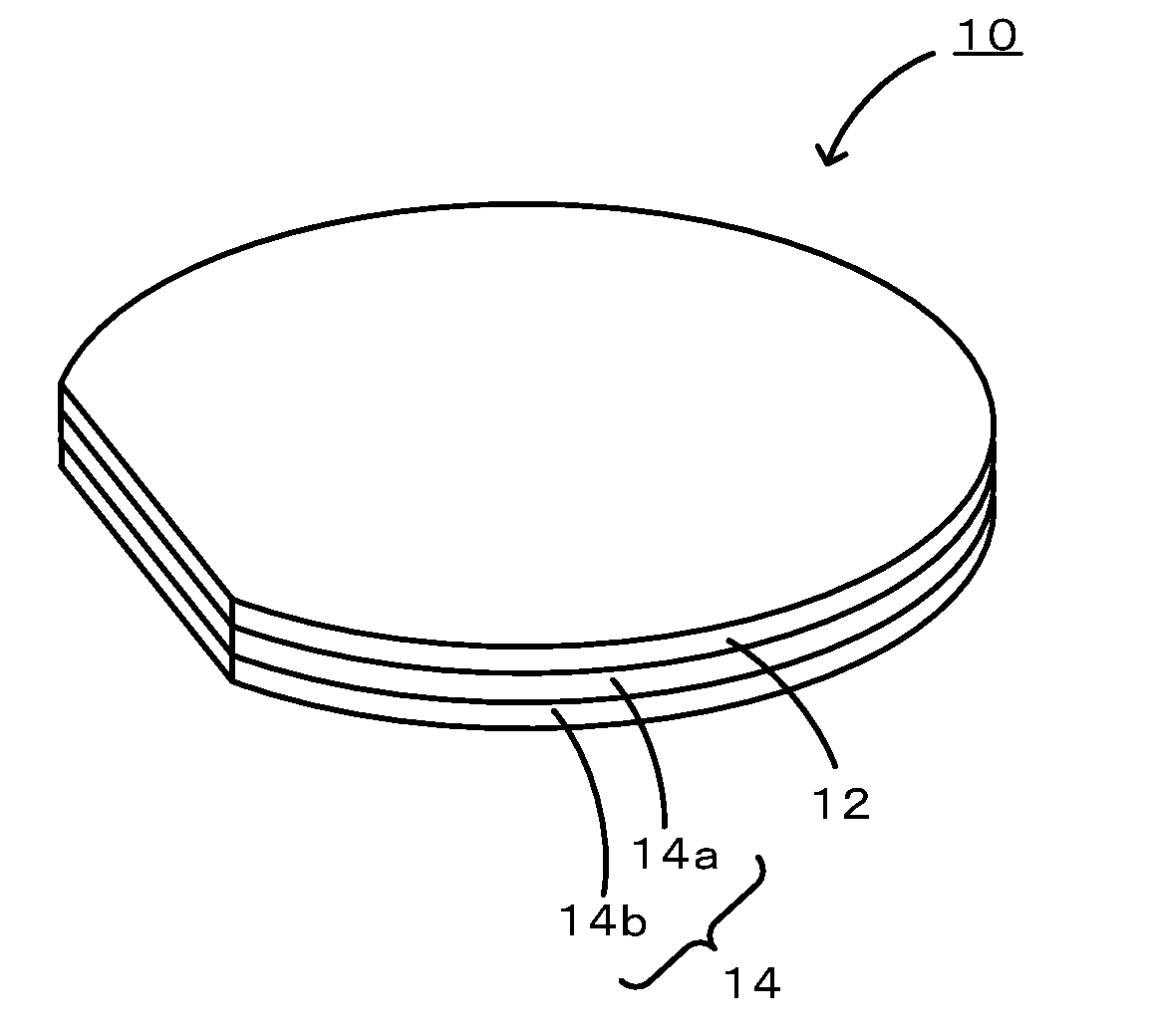
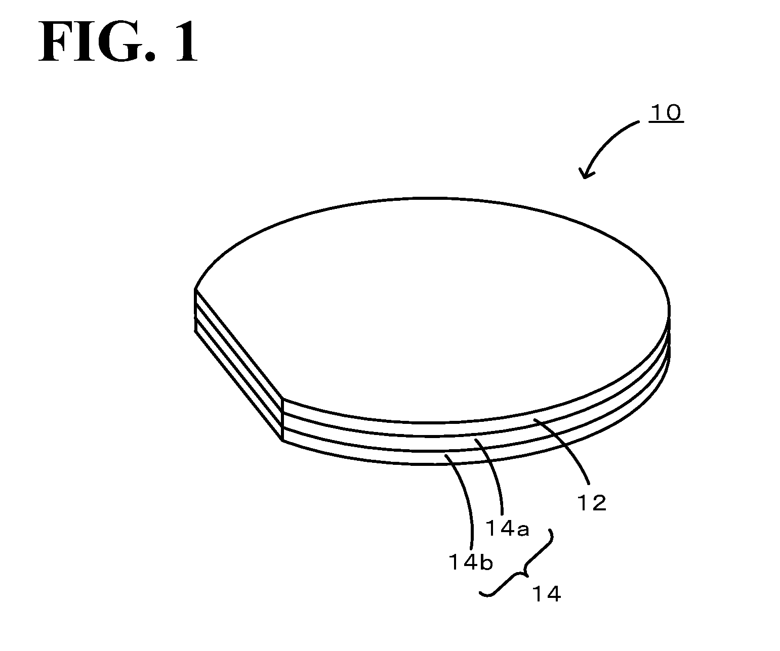
[0040]Two silicon substrates having a diameter of 100 mm and a thickness of 250 μm were prepared as first and second substrates. Each silicon substrate prepared had two mirror-finished surfaces. Each silicon substrate was washed to remove foreign matter from the surfaces and subsequently introduced into a vacuum chamber formed of stainless steel. The atmosphere within the chamber was adjusted to a vacuum on the order of 1×10⁻⁶ Pa. Within this atmosphere, a surface of each silicon substrate was irradiated with Ar ion beams for 180 sec. Subsequently, the beam-irradiated surfaces of the silicon substrates were overlapped so as to be in contact with each other and a load of 500 kgf was then applied to bond together the silicon substrates. Thus, a support substrate having a total thickness of 500 μm was obtained. In addition to this support substrate, a LT substrate having two mirror-finished surfaces, a diameter of 100 mm, and a thickness of 230 μm was prepared as a piezoelectric substr...

example 2

[0045]The polished composite substrate in Example 1 was subjected to patterning for electrodes for elastic wave devices (surface acoustic wave devices). A blade was then inserted into the Si—Si bonding boundary to divide the bonded substrate. This provided a bilayer composite substrate in which the LT substrate and the Si substrate (first substrate) were bonded together and a monolayer Si substrate (second substrate). The separated surface of the bilayer composite substrate and the separated surface of the monolayer Si substrate were observed with an AFM (atomic force microscope). As a result, the wafers were found to have a surface roughness Ra of about 0.4 nm and the surfaces were in a good condition without the need of polishing. The separated surfaces were subjected to elemental analysis by energy dispersive X-ray spectrometry (EDS). As a result, in addition to the Si element, the Fe element and the Cr element were detected. The Fe element and the Cr element were derived from th...


PUM

PropertyMeasurementUnit
thicknessaaaaaaaaaa
thicknessaaaaaaaaaa
thicknessaaaaaaaaaa

Abstract

A composite substrate 10 is formed by bonding together a piezoelectric substrate 12 and a support substrate 14 that has a lower thermal expansion coefficient than the piezoelectric substrate. The support substrate 14 is formed by directly bonding together a first substrate 14a and a second substrate 14b at a strength that allows separation with a blade, the first and second substrates being formed of the same material, and a surface of the first substrate 14a is bonded to the piezoelectric substrate 12, the surface being opposite to another surface of the first substrate 14a bonded to the second substrate 14b.

Description

BACKGROUND OF THE INVENTION[0001]1. Field of the Invention[0002]The present invention relates to a composite substrate, an elastic wave device, and a method for producing an elastic wave device.[0003]2. Description of the Related Art[0004]In recent years, for the purpose of improving the temperature characteristics of elastic wave devices, a composite substrate formed by bonding a thin piezoelectric substrate onto a support substrate having a low thermal expansion coefficient is used. For example, Patent Literature 1 discloses a composite substrate having a structure formed by bonding together a LT substrate (LT is the abbreviation of lithium tantalate) serving as a piezoelectric substrate and a silicon substrate serving as a support substrate via an adhesive layer formed of an epoxy adhesive.[0005]Production of elastic wave devices with such a composite substrate has the following problems. First, since the composite substrate warps considerably in response to changes in temperatur...

Claims


Application Information

Patent Timeline
Patent Type & Authority Applications(United States)
IPC IPC(8): B32B38/10H03H9/25B32B7/02H01L41/187B32B9/00B32B9/04B32B7/025
CPCB32B38/10B32B9/005B32B9/04Y10T428/12597H01L41/1873H03H9/25B32B2457/00B32B7/02H03H3/10H03H9/02574B32B7/12B32B27/08B32B27/20B32B27/283B32B2264/105B32B2307/20B32B2307/538B32B37/10B32B2309/02B32B2309/105H03H3/08B32B2457/14B32B7/025H10N30/072Y10T29/49005Y10T29/42H03H2003/023H03H2003/027H03H2003/022H03H3/02H03H9/1014H03H9/1035H03H9/105H10N30/8542B32B7/06B32B18/00B32B2307/206H01L21/6835H01L21/78
Inventor HATTORI, RYOSUKEHORI, YUJITAI, TOMOYOSHI
Owner NGK INSULATORS LTD
Why Eureka
Try Eureka