Correcting for stress induced pattern shifts in semiconductor manufacturing

a semiconductor and stress-induced pattern technology, applied in the field of semiconductor chip manufacturing, can solve problems such as overlay errors between dt and rx shapes, overlay errors between mask layers, and systemic stress, and achieve the effect of reducing overlay errors

Active Publication Date: 2015-12-17
GLOBALFOUNDRIES US INC
View PDF1 Cites 11 Cited by
  • Summary
  • Abstract
  • Description
  • Claims
  • Application Information

AI Technical Summary

Benefits of technology

[0012]In one aspect, a method of reducing overlay errors during a semiconductor photolithographic mask design process flow is described. The method comprises: obtaining data representing density characteristics of a photo mask layout design; predicting stress induced displacements based on the obtai...

Problems solved by technology

Stress impacts the performance of semiconductor devices by altering the band structure of the semiconductor material, and consequently, the mobility of carriers.
As stress effects in silicon processing cause displacements in the silicon lattice in intermediate stages of silicon processing, these displacements may cause overlay error between mask layers.
For example, during the manufacture of embedded DRAM layouts, there can be overlay errors between DT and RX shapes (where DT is a deep trench and RX recessed oxide), induced during the annealing of deep trench structures.
The displac...

Method used


Image

  • Correcting for stress induced pattern shifts in semiconductor manufacturing
  • Correcting for stress induced pattern shifts in semiconductor manufacturing
  • Correcting for stress induced pattern shifts in semiconductor manufacturing

Examples


Embodiment Construction

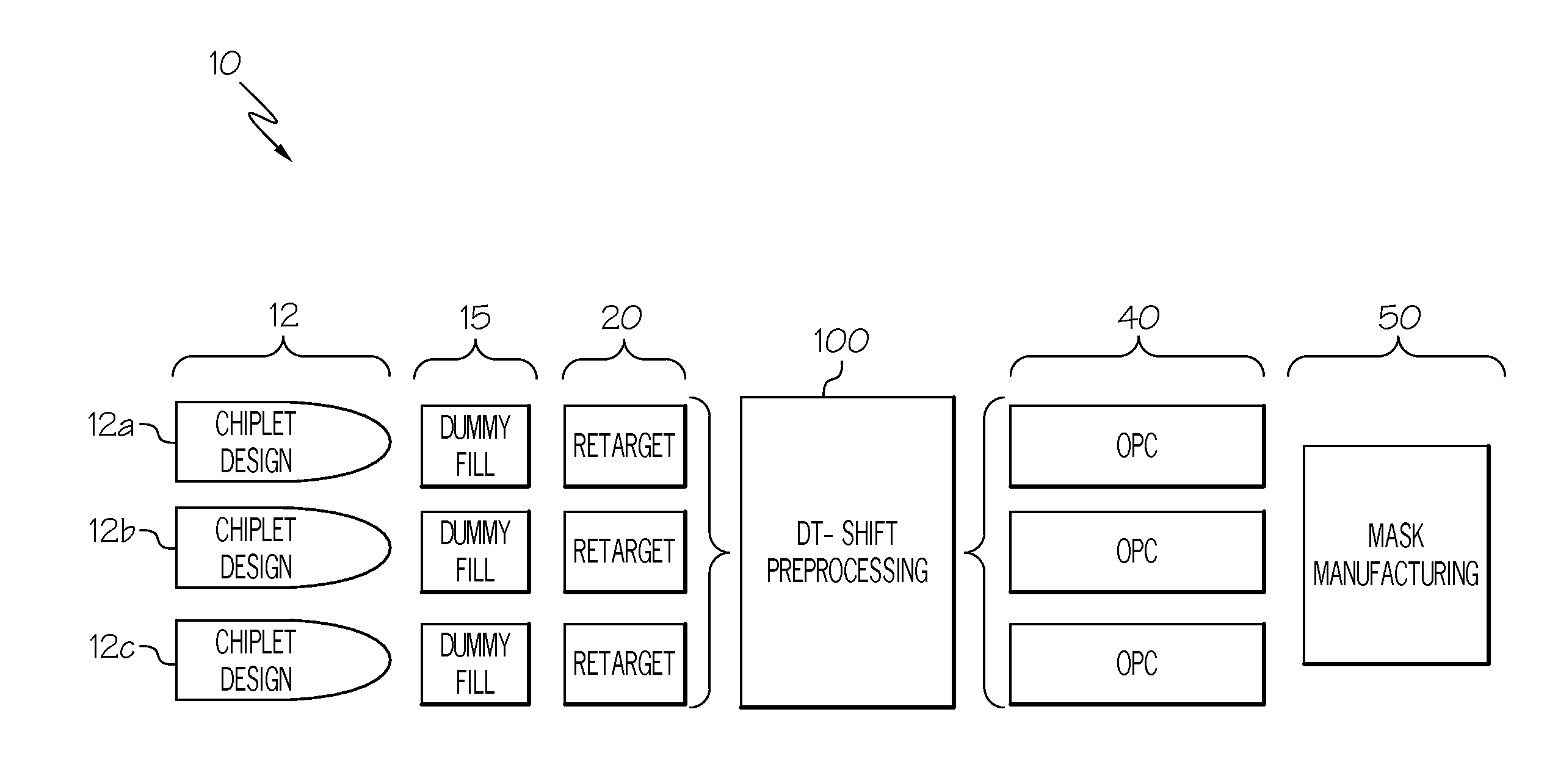
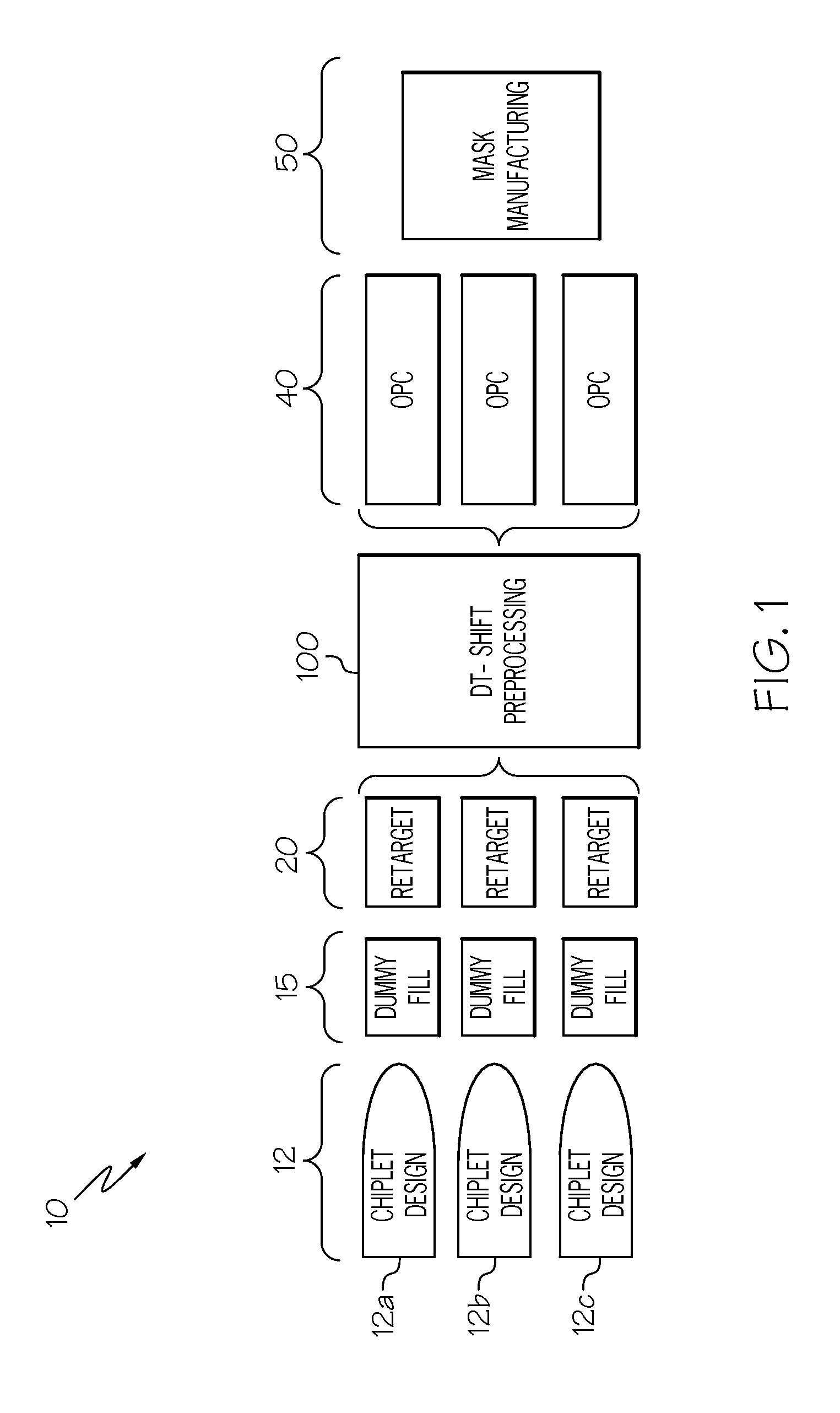
[0019]The present disclosure describes a system and method for reducing overlay error by 1) modeling stress induced displacements based on knowledge of density characteristics of layout, and 2) using this model to correct mask data by moving individual shapes in the mask data in a manner to pre-compensate for expected shifts.

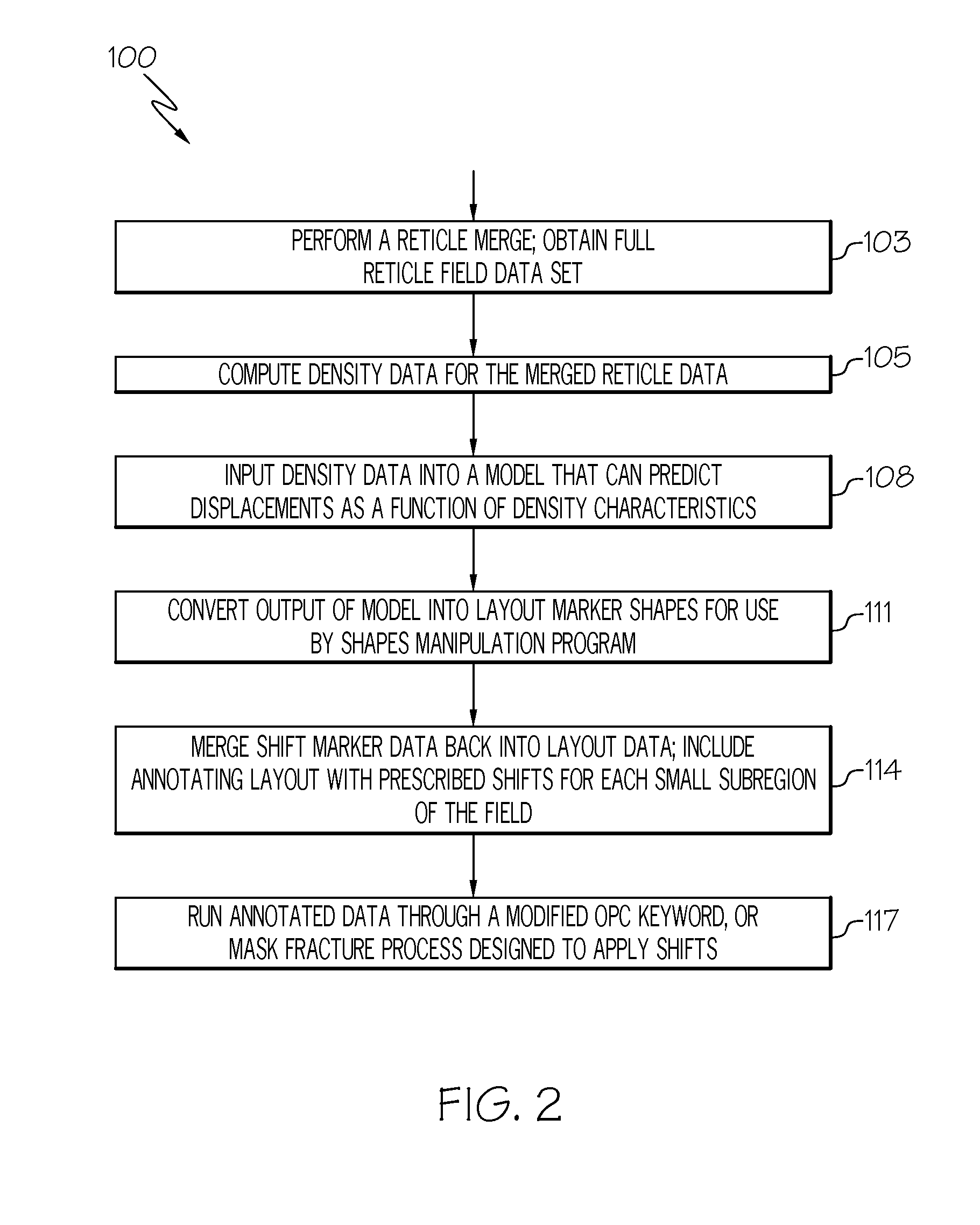
[0020]As one embodiment of method there is performed steps that: 1) perform a reticle merge where density characteristic driven stress effect are merged into a full reticle field data set; 2) compute density data for the merged reticle data; 3) use density data as an input into a model that may predict displacements as a function of density; 4) convert predicted shift data into layout marker data; 5) merge shift marker data back into layout data thereby effectively annotating the layout with prescribed shifts for each small sub-region of the field; and 6) run annotated data through a modified OPC recipe or mask fracture process that are designed to apply displac...


PUM


Abstract

Apparatus, method and computer program product for reducing overlay errors during a semiconductor photolithographic mask design process flow. The method obtains data representing density characteristics of a photo mask layout design; predicts stress induced displacements based on said obtained density characteristics data; and corrects the mask layout design data by specifying shift movement of individual photo mask design shapes to pre-compensate for predicted displacements. To obtain data representing density characteristics, the method merges pieces of data that are combined to make a photo mask to obtain a full reticle field data set. The merge includes a merge of data representing density characteristic driven stress effects. The density characteristics data for the merged reticle data are then computed. To predict stress-induced displacements, the method inputs said density characteristics data into a programmed model that predicts displacements as a function of density, and outputs the predicted shift data.

Description

FIELD OF INVENTION[0001]This disclosure relates generally to the manufacture of semiconductor chips devices and structures, and a novel system and method to correct for stress induced pattern shifts and distortions in semiconductor manufacturing such as by correcting for localized overlay errors by correcting mask data during the mask data processing flow.BACKGROUND[0002]Stress impacts the performance of semiconductor devices by altering the band structure of the semiconductor material, and consequently, the mobility of carriers. This effect is prominent in many semiconductor devices, e.g., metal-oxide-semiconductor field effect transistor (MOSFET) devices. For example, minority carriers in the body, e.g., hole mobility of a p-type MOSFET, formed on a silicon substrate increases under a uniaxial compressive stress in the direction of the channel, i.e., along a line connecting the source and the drain, thereby impacting transconductance of a MOSFET. The electron mobility of an n-type...

Claims


Application Information

Patent Timeline
IPC IPC(8): G06F17/50
CPCG06F17/5081H01L27/0207G03F7/70433G03F7/70633
Inventor CHIDAMBARRAO, DURESETICULP, JAMES A.PARRIES, PAUL C.STOBERT, IAN P.
Owner GLOBALFOUNDRIES US INC
Why Eureka
Try Eureka