Composite Structure of Tungsten Copper and Molybdenum Copper with Embedded Diamond for Higher Thermal Conductivity

a technology of molybdenum copper and molybdenum copper, which is applied in the field of packaging semiconductor devices, can solve the problems of reducing the life of the die/device, poor reliability, and generating substantial heat in the semiconductor and laser die, so as to increase the power gain, and increase the overall physical size of the system

Inactive Publication Date: 2016-01-07
THERMAL MANAGEMENT SOLUTIONS LLC D B A SANTIER
View PDF0 Cites 18 Cited by
  • Summary
  • Abstract
  • Description
  • Claims
  • Application Information

AI Technical Summary

Benefits of technology

[0010]The second key advantage of Cu—Mo composite is that it is more transparent to x-rays. Many manufacturers of electronic devices prefer to inspect their devices by x-ray imaging after they are sealed. Tungsten is much more opaque to x-rays than molybdenum, and the type of x-ray imaging machines normally used in this type of inspection cannot see through Cu—W, but they can see through Cu—Mo.
[0012]When the same copper-molybdenum laminate material is embedded with copper diamond the resultant change in thermal conductivity in the through plane is approximately 600-700 W / mK and in plane thermal conductivity is also at approximately 600-700 w / mK in the region which is embedded by Cu-diamond. This change in fundamental thermal property of the heat sink can help run a semiconductor laser die 10 degree Celsius or more cooler. This can help in increasing performance of the overall system without increasing the system's overall physical size. Also it can help increase the power gain from the GaN power amplifier design by +2 dB or more, which is a power amplification gain of over 58.5% from input to output.

Problems solved by technology

Semiconductor and laser dies generate substantial amount of heat due to long duty cycles.
Failure to meet both of these requirement results into poor reliability and reduces the life of the die / devices.

Method used


Image

  • Composite Structure of Tungsten Copper and Molybdenum Copper with Embedded Diamond for Higher Thermal Conductivity
  • Composite Structure of Tungsten Copper and Molybdenum Copper with Embedded Diamond for Higher Thermal Conductivity
  • Composite Structure of Tungsten Copper and Molybdenum Copper with Embedded Diamond for Higher Thermal Conductivity

Examples


Embodiment Construction

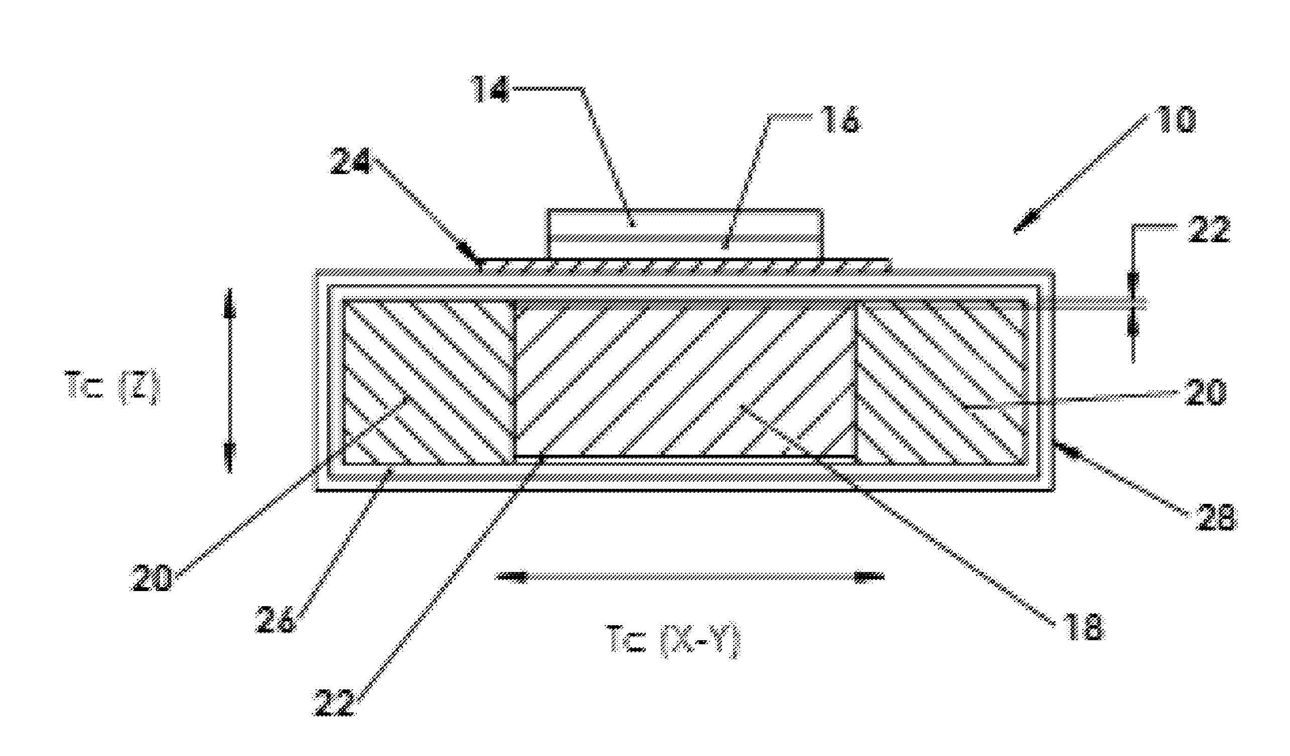
[0018]The following steps outline one embodiment of a method to manufacture a composite structure that will provide high thermal conductivity in the X and Y plane of the layers, as well as through plane (Z-axis).

[0019]The first step is to press and first pass sinter a tungsten or molybdenum preform 20 of known porosity, and to machine, such as by milling, drilling, grinding or, punching a through cavity in the preform 20. The preform 20 is preferably a rectangular solid, with a rectangular cavity, thus comprising a “window frame” configuration. Then, the preform 20 is etched with a suitable etchant to achieve the desired surface porosity.

[0020]The second step is to embed a unitary insert of porous synthetic [or natural] isotropic diamond material 18 into the cavity, making sure that the upper surface of the diamond material is slightly lower than the top height of the cavity, thus forming a gap 22. The gap in the surface of the diamond material is preferably 0.002 to 0.004 inches be...


PUM

PropertyMeasurementUnit
melting temperatureaaaaaaaaaa
lengthaaaaaaaaaa
heataaaaaaaaaa

Abstract

A heatsink for dissipating heat generated by electronic components comprising an outer frame of copper tungsten or copper molybdenum metal matrix composite having a cavity extending between the top and the bottom surfaces, a copper-diamond composite material within the opening, and copper plating on the top and the bottom surfaces. The heatsink also includes an array of alternating layers of copper and a material selected from the group of molybdenum and copper / molybdenum metal matrix surrounding the outer frame. The heatsink can be manufactured by press fitting at room temperature a porous isotropic diamond material in the cavity of an outer frame of porous tungsten or molybdenum, co-infiltrating the assembly under pressure with copper, press fitting at room temperature the outer frame into the layered array, and subjecting the heatsink to a temperature of approximately 800 Deg C.

Description

CROSS-REFERENCE TO RELATED APPLICATIONS[0001]This application claims priority to provisional application 62 / 015,469, filed Jun. 22, 2014 and provisional application 62 / 144,679, filed Apr. 8, 2015.FIELD OF THE INVENTION[0002]The invention relates to the field of packaging semiconductor devices. In particular, the invention relates to the field of hermetic, non-organic packaging of high power and / or high frequency semiconductor devices. More particularly, the invention relates to hermetic and non-hermetic packages that are closely matched to the coefficient of thermal expansion of the semiconductor / Laser devices mounted thereupon and that provide a thermally conductive pathway for heat dissipation.BACKGROUND OF THE INVENTION[0003]Much of the semiconductor packaging currently in use in the electronics industry is produced from organic laminate materials; however, there still exists a need for hermetic and non hermetic, non-organic-based packaging for high power, high operating temperat...

Claims


Application Information

Patent Timeline
Patent Type & Authority Applications(United States)
IPC IPC(8): B23P15/26F28F21/08H05K7/20
CPCF28F21/085B23P15/26H05K7/20509H01L23/34H01L23/3732H01L23/3735H01L23/3736H01L2924/0002F28F21/00F28F21/08H01L2924/00
Inventor DUTTA, SANCHAYAN
Owner THERMAL MANAGEMENT SOLUTIONS LLC D B A SANTIER
Why Eureka
Try Eureka