Process for making triple graded CVC-CVD-CVC silicon carbide products

a silicon carbide and triple grade technology, applied in the field of stress-free, thermally stable silicon carbide (sic) composites, can solve the problems of high manufacturing and fabrication costs of lightweighted optics, high toxic and expensive procurement and fabrication, and polished surfaces, etc., to achieve precise optical prescriptions, easy grounding and polishing, and high purity

Inactive Publication Date: 2016-01-28
BOLTON LAUREN
View PDF0 Cites 6 Cited by
  • Summary
  • Abstract
  • Description
  • Claims
  • Application Information

AI Technical Summary

Benefits of technology

[0024]The present invention provides a chemical vapor composite deposition process for fabricating low stress, thermally stable, highly polishable silicon carbide products. In preferred embodiments a graphite substrate is prepared having the desired shape of the resultant silicon carbide deposit. The substrate is placed in a high temperature chemical vapor reactor. Three layers of silicon carbide are vapor deposited on the graphite substrate. The first layer is a sacrificial layer, deposited using the chemical vapor composite (CVC) process in which an aerosol of solid micron-scale SiC particles is entrained within a reactant chemical vapor precursor and injected into the high temperature reactor to form a high purity, solid CVC SiC foundation upon which the second and third layers will be deposited. The second layer is a highly polishable CVD SiC material that is formed by continuous deposition of the high purity chemical precursors, but without the solid silicon carbide particles. This second layer is thin and thus not plagued by the inherent stress of bulk CVD SiC. Moreover, because it is deposited on top of a stress-free CVC SiC foundation, with an identical coefficient of thermal expansion, any tensile stress in the CVD layer would be further reduced. These stress mitigation design strategies result in a second layer of SiC material that can be easily ground and polished to precise optical prescriptions. The third layer comprises the bulk of the mirror structure and is deposited using the CVC SiC process. It is formed by continuous deposition of the high purity chemical precursors and resuming the incorporation of the micron-scale solid silicon carbide particles. The third layer can be as thick as needed to meet the geometric, strength and structural requirements of the product's design. Since deposition of the three layers is absolutely continuous (no change in gas flow rates, temperature or pressure) the grain structure of each layer transitions seamlessly into the next (confirmed by microscopic evaluation).

Problems solved by technology

The extensive amount of machining required to lightweight a mirror, compounded by the amount of bulk material that is ultimately unused, makes the manufacturing and fabrication costs of lightweighted optics very high.
Beryllium (Be) has been utilized extensively in airborne optics, however it is highly toxic and expensive to procure and fabricate.
Although CVC SiC optics polish extremely well the polished surface has been observed, on rare occasions, to have micron scale imperfections.
Particle pull-out results in a microscopic void (dig) in the mirror's optical surface.
Such surface defects may result in light scattering, undesired diffraction patterns, loss of contrast and stray light, which can degrade image quality and affect overall optical system performance.
While the occurrence of particle pull out is rare, the potential result can be significant.

Method used


Image

  • Process for making triple graded CVC-CVD-CVC silicon carbide products
  • Process for making triple graded CVC-CVD-CVC silicon carbide products
  • Process for making triple graded CVC-CVD-CVC silicon carbide products

Examples


Embodiment Construction

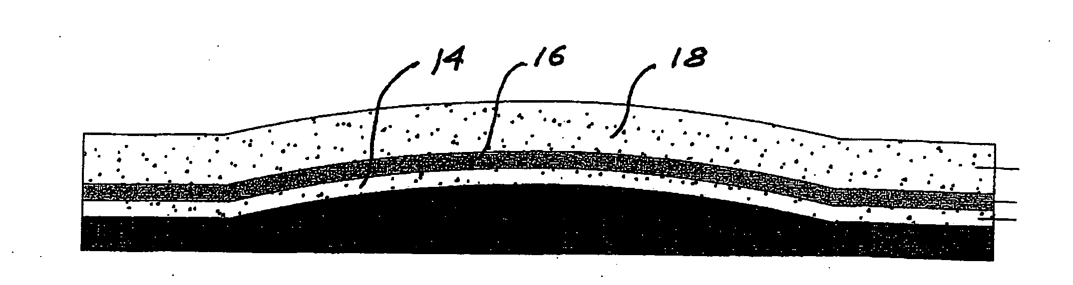
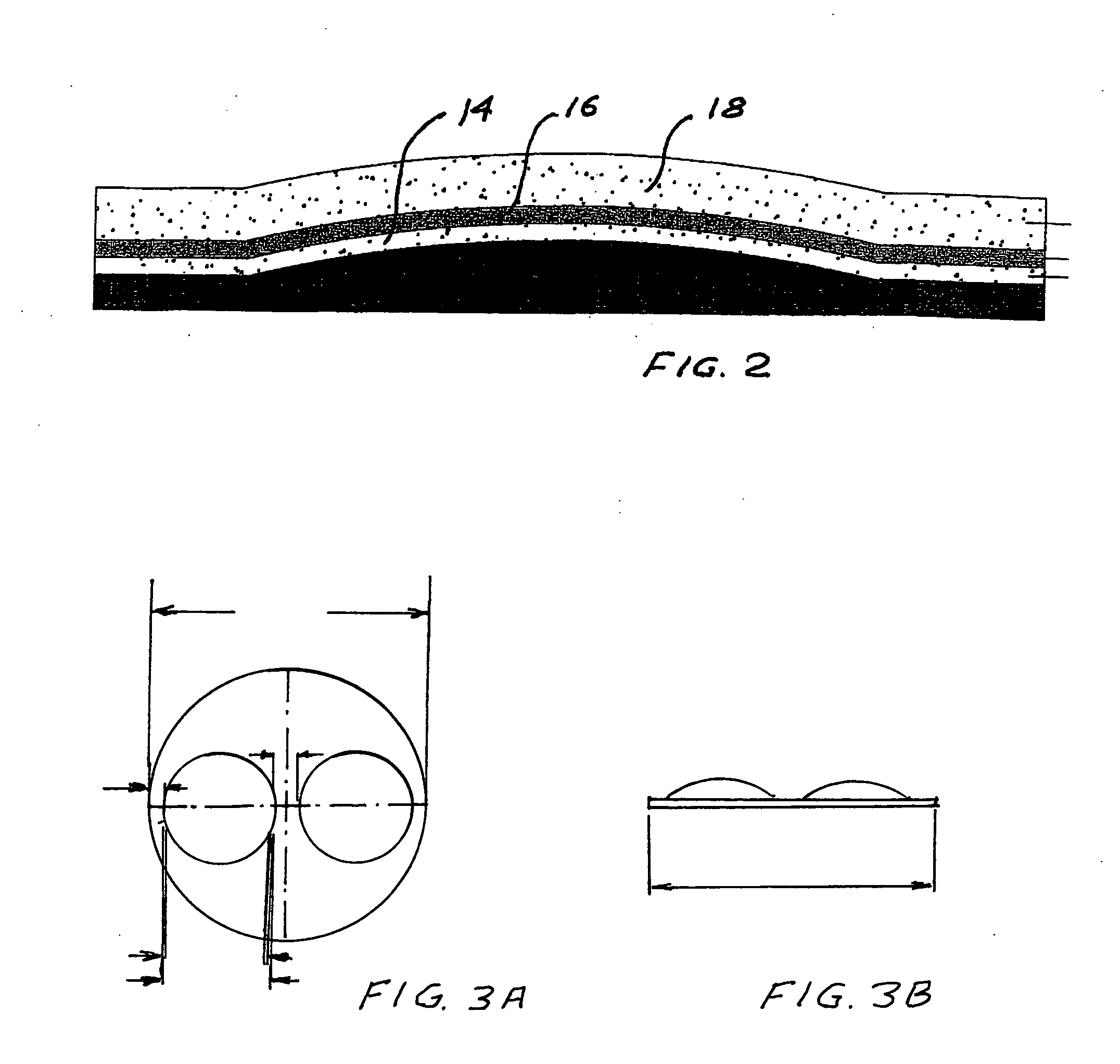
Applicant's CVC-CVD-CVC Process

[0032]As explained in the background section, Applicant's employer has developed, patented and trademarked its CVC process for making stress-free, thermally stable, high purity silicon carbide products. CVD processes are well known and similar to the Applicant's CVC process except that micron-scale solid particles are not used in CVD silicon carbide. The present invention marries the superior optical and thermo-mechanical properties of CVD SiC and the virtually stress-free grain structure of CVC SiC to produce silicon carbide products far superior to products produced by CVD alone.
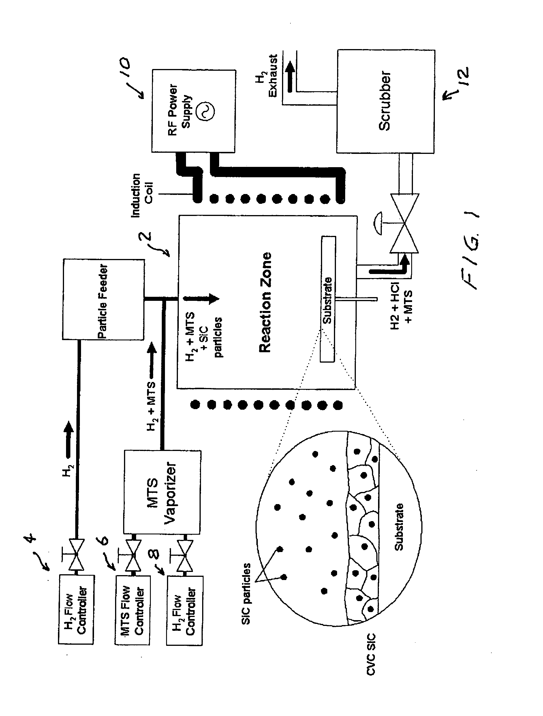
The CVC Process

[0033]To make CVC SiC an aerosol of solid micron-scale SiC particles is entrained within a reactant chemical vapor precursor and injected into a high temperature furnace. The aerosol mixture reacts at high temperature to form high purity solid CVC SiC on a heated graphite substrate. The chemical process is analogous to chemical vapor deposition (CVD), which sim...


PUM

PropertyMeasurementUnit
melting pointaaaaaaaaaa
surface roughnessaaaaaaaaaa
aspect ratioaaaaaaaaaa

Abstract

A chemical vapor composite process for making high quality silicon carbide suitable for optical and structural components with low intrinsic stress and high thermal stability. In the CVC process solid micron-scale silicon carbide particles are incorporated into a high purity chemical vapor stream and injected into a high temperature furnace. Three layers of silicon carbide are vapor deposited on the graphite mandrel. The first layer is a sacrificial layer, deposited utilizing the chemical vapor composite process. The second layer is the optical cladding CVD layer, which is deposited by continuous deposition of the high purity chemical precursor without the silicon carbide particles. This layer is ground and polished to a high optical finish. The third layer is the bulk of the mirror structure and deposited via the CVC SiC process as described above. The thickness of this structural layer is determined by the product's geometrical and structural requirements.

Description

FEDERAL SUPPORTED RESEARCH[0001]The present invention was made in the course of work under contract Number HQ0006-05-D-0006 and the United States Government has rights in the invention.FIELD OF THE INVENTION[0002]The present invention relates to stress-free, thermally stable silicon carbide (SiC) composites, and in particular to SiC composite optics (mirrors).BACKGROUND OF THE INVENTIONSilicon Carbide[0003]Silicon carbide, also known as carborundum, is a rare earth element, existing naturally in minute quantities only in the form of moissanite in certain types of meteorites and corundum deposits and kimberlite. Virtually all the silicon carbide sold in the world is synthetic. Early experiments in the synthesis of silicon carbide were conducted during the 1800's using a variety of source materials and processes. Wide scale production of silicon carbide as we know it today is credited to Edward Goodrich Acheson in 1890. Acheson patented the method for making silicon carbide powder and...

Claims


Application Information

Patent Timeline
Patent Type & Authority Applications(United States)
IPC IPC(8): C23C16/32C23C16/01
CPCC23C16/01C23C16/325C23C16/4417G02B5/0833G02B5/10
Inventor BOLTON, LAUREN
Owner BOLTON LAUREN
Why Eureka
Try Eureka