

Vanadium oxide thermo-sensitive film material with high temperature coefficient of resistance and a preparing method thereof
a technology of thermo-sensitive film and vanadium oxide, which is applied in the field of infrared detectors and electronic materials, can solve the problems of poor resistance stability of this kind of mixed-valence vanadium oxide film, the difficulty of mems-process compatibility of manufacturing ufpas, and the difficulty of thermo-sensitive film preparation
- Summary
- Abstract
- Description
- Claims
- Application Information
AI Technical Summary
Benefits of technology
Problems solved by technology
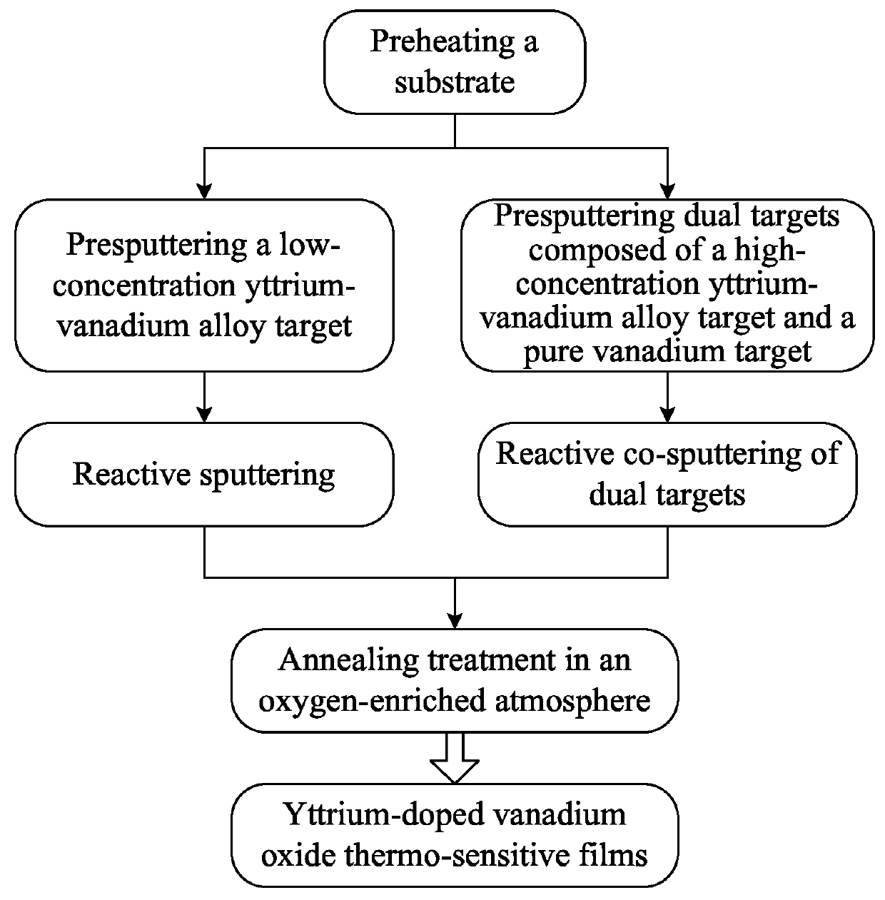
Method used
Image

Examples
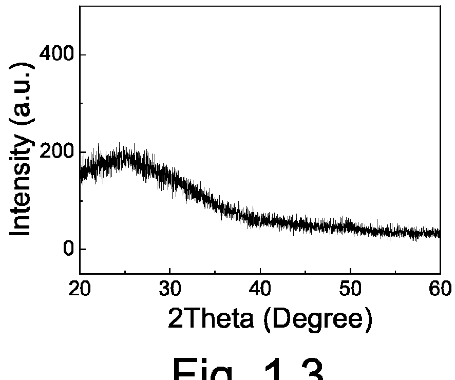
example 1.1
[0038]A silicon wafer having a film of 300 nm SiNx is preheated at 200° C. for 60 minutes in a sputtering chamber under a vacuum environment. Under an atmosphere of an oxygen / argon flow ratio of 1:20, a low-concentration yttrium-vanadium alloy target with a yttrium atomic concentration of 5.0% is pre-sputtered for 5 minutes at a working pressure of 1.5 Pa. Then under an atmosphere of an oxygen / argon flow ratio of 1:20, the pre-sputtered low-concentration yttrium-vanadium alloy target is sputtered and the yttrium-doped vanadium oxide film is deposited on the preheated silicon wafer with a film of 300 nm SiNx for 25 minutes. Then in an oxygen-enriched atmosphere with an oxygen / argon flow ratio of 1:0.2 and at a working pressure of 2.0 Pa, the deposited yttrium-doped vanadium oxide film is annealed for 100 minutes at 250° C. After the annealing treatment is finished, temperature is dropped to 100° C. below. Samples (denoted as VYO-11) are taken out for measurement.
[0039]Meanwhile, as a...
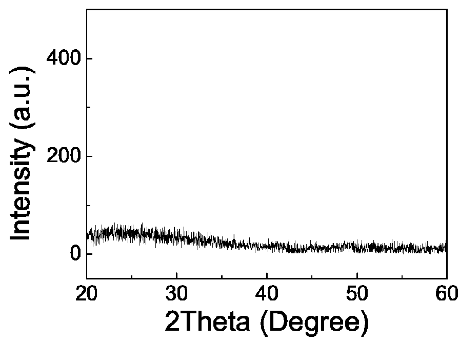
example 1.2
[0049]A silicon wafer having a film of 300 nm SiNx is preheated at 100° C. for 30 minutes in a sputtering chamber under a vacuum environment. Under an atmosphere of an oxygen / argon flow ratio of 1:15, a low-concentration yttrium-vanadium alloy target with a yttrium atomic concentration of 2.0% is pre-sputtered for 3 minutes at a working pressure of 0.5 Pa. Then under an atmosphere of an oxygen / argon flow ratio of 1:20, the pre-sputtered low-concentration yttrium-vanadium alloy target is sputtered and the yttrium-doped vanadium oxide film is deposited on the preheated silicon wafer with a film of 300 nm SiNx for 25 minutes. Then in an oxygen-enriched atmosphere with an oxygen / argon flow ratio of 1:1 and at a working pressure of 0.5 Pa, the deposited yttrium-doped vanadium oxide film is annealed for 30 minutes at 150° C. After the annealing treatment is finished, temperature is dropped to 100° C. below. Samples (denoted as VYO-12) are taken out for measurement.
[0050]Meanwhile, as a co...
example 1.3
[0056]A silicon wafer having a film of 300 nm SiNx is preheated at 250° C. for 150 minutes in a sputtering chamber under a vacuum environment. Under an atmosphere of an oxygen / argon flow ratio of 1:30, a low-concentration yttrium-vanadium alloy target with a yttrium atomic concentration of 12.0% is pre-sputtered for 10 minutes at a working pressure of 2.0 Pa. Then under an atmosphere of an oxygen / argon flow ratio of 1:30, the pre-sputtered low-concentration yttrium-vanadium alloy target is sputtered and the yttrium-doped vanadium oxide film is deposited on the preheated silicon wafer with a film of 300 nm SiNx for 25 minutes. Then in an oxygen-enriched atmosphere with an oxygen / argon flow ratio of 1:0 and at a working pressure of 3.0 Pa, the deposited yttrium-doped vanadium oxide film is annealed for 150 minutes at 280° C. After the annealing treatment is finished, temperature is dropped to 100° C. below. Samples (denoted as VYO-13) are taken out for measurement.
[0057]Meanwhile, as ...
PUM
| Property | Measurement | Unit |
|---|---|---|
| Fraction | aaaaa | aaaaa |
| Fraction | aaaaa | aaaaa |
| Fraction | aaaaa | aaaaa |
Abstract
Description
Claims
Application Information