A junction-modulated tunneling field effect transistor and a fabrication method thereof

a field effect transistor and junction-modulated technology, applied in the direction of diodes, semiconductor devices, electrical apparatus, etc., can solve the problems of increasing the power consumption of devices, increasing the active area of devices, and increasing the negative effect of devices such as short channel effects, so as to improve the effective tunneling area, improve the sub-threshold characteristics, and not increase the active area of the active region

Inactive Publication Date: 2016-03-17
PEKING UNIV
View PDF0 Cites 6 Cited by
  • Summary
  • Abstract
  • Description
  • Claims
  • Application Information

AI Technical Summary

Benefits of technology

[0020]Firstly, the PN junction provided by a highly-doped source region surrounding three sides of the vertical channel region of the tunneling field effect transistor of the present invention can deplete effectively the channel region, so that energy band of the surface channel under the gate is lifted, therefore the device may obtain a steeper energy band and a narrower tunneling barrier width than the conventional TFET when the band-to-band tunneling occurs, equivalently achieving the effect of a steep doping concentration gradient at the tunneling junction, and thereby the sub-threshold characteristics are significantly improved relative to the conventional TFET. At the same time, compared with a junction-depletion-mode tunneling field effect transistor with a planar strip-shaped gate, the three sides-surrounding structure of the present invention can modulate more effectively the tunneling junction to obtain the steeper sub-threshold characteristics, because depletion is caused by only the PN junctions on the two sides with respect to a planar structure.
[0021]Secondly, on the premise of not increasing the area of the active region, the design of the vertical channel region of the present invention can improve effectively the tunneling area which is determined by the area of the interface between the highly-doped source region and gate, as shown by the section outlined by a dashed box in FIG. 1a. The increase in the tunneling area can be benefit to further improve the on-state current of the device.
[0022]Thirdly, the present invention adopts a short gate design, that is, the gate electrode covers a part of the channel region so that there is an uncovered region of a certain distance between the gate and the drain. The design not only can inhibit effectively the tunneling at the drain junction, that is, the ambipolar effect in the conventional TFET, but also can reduce the influence of the gate electrode on the uncovered region and accordingly can inhibit the tunneling of the parasitic tunneling junction in a small size device, the place where the parasitic tunneling junction occurs is the location indicated by a point B in FIG. 1a. Therefore, the sub-threshold slope of the device may be decreased when the device is turned on. In addition, the lower doping concentration of the drain region may also further inhibit the ambipolar effect.
[0023]Fourthly, the fabrication process of the device is simple, and the fabrication method is fully compatible with the conventional MOSFET process.
[0024]In short, the tunneling area of the device is increased due to application of the vertical channel region to the device structure, the application of the design of the highly-doped source region surrounding the channel region on three sides modulates effectively the tunneling junction at the source, and inhibits the ambipolar effect and the tunneling of the parasitic tunneling junction in the small size device, improving the on-state current and the sub-threshold characteristics of TFET device, and the fabricating method is simple. Compared with the existing TFET, in the case of the same active region size, the device of the present invention can obtain a higher turn-on current and a steeper sub-threshold slope, and can maintain a lower leakage current, and thus the device can be expected to be applied in the field of the low power consumption, and has a higher practical value.

Problems solved by technology

Under the drive of Moore's Law, the feature size of the conventional MOSFET continually shrink and now has progressed to the nanometer scale, consequently, the negative effects such as short channel effect of a device and so on have become increasingly critical.
The effects such as drain induced barrier lowering and band-to-band tunneling cause a off-state leakage current of a device to increase continually, and at the same time, a sub-threshold slope of the conventional MOSFET can not decrease synchronously with the shrink of the device size due to the limitation by the thermal potential, and thereby result in increase of the device power consumption.
Now the power consumption concern has become the most serious problem of limiting the device shrink.
However, due to the limitation of source junction tunneling probability and tunneling area, TFET is faced with an issue of small on-state current, which is far less than the conventional MOSFET devices, and this greatly limits the applications of TFET device.
In addition, it is difficult to achieve TFET device with a steep sub-threshold slope in the experiment, because it is more difficult to achieve a steep doping concentration gradient at the source junction in the experiment, so that the electric field at the tunneling junction when the device turns on is not sufficiently large, which may cause a sub-threshold slope of TFET to degrade relative to the theoretical value.
Therefore, it has become a further important problem in connection with TFET device how to achieve a steep doping concentration gradient at the source junction so as to obtain an ultra-low sub-threshold slope.

Method used


Image

  • A junction-modulated tunneling field effect transistor and a fabrication method thereof
  • A junction-modulated tunneling field effect transistor and a fabrication method thereof
  • A junction-modulated tunneling field effect transistor and a fabrication method thereof

Examples


Embodiment Construction

[0033]Hereinafter, the present invention will be further described with respect to the examples. It is noted that, the embodiments are provided so that this disclosure will be thorough and complete, and will fully convey the scope of the present invention to those skilled in the art, and it will be appreciated to those skilled in the art that various changes and modifications may be made without departing from the spirit and scope defined by the present invention and the accompanying claims. Accordingly, the present invention should not be construed as being limited to the embodiments, and the protected scope of the present invention should be defined by the claims.

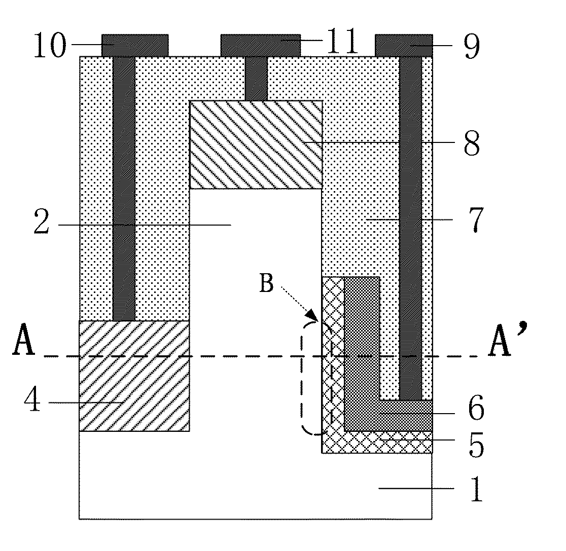
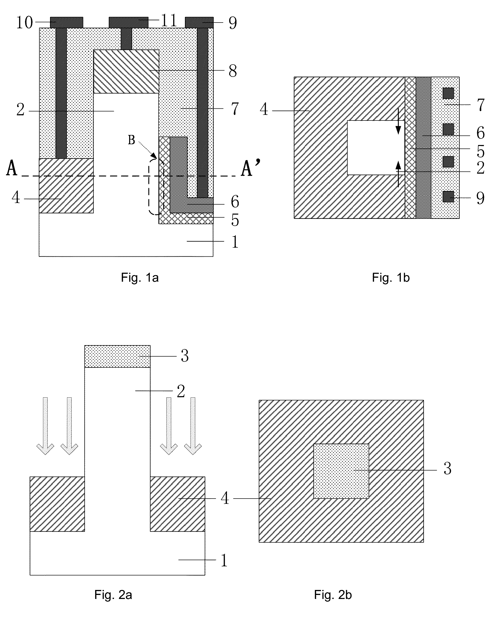
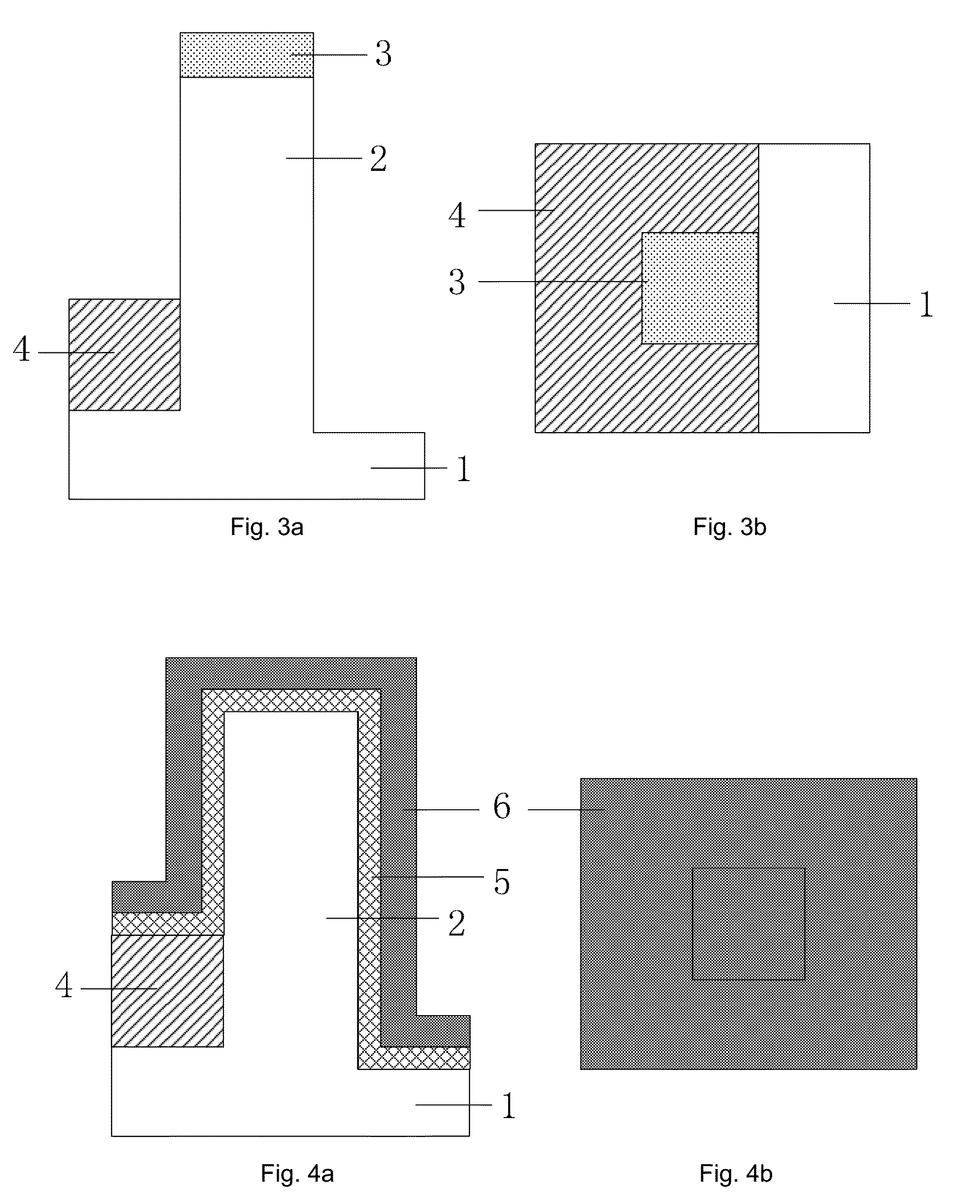
[0034]A specific example of the fabrication method according to the present invention includes the process steps shown in FIG. 2 to FIG. 7:

[0035]1. A hard mask layer 3 is deposited on a silicon substrate 1 in the form of a bulk silicon wafer with a crystal orientation (100), wherein the hard mask layer is Si3N4 and has a ...


PUM


Abstract

The present invention discloses a junction-modulated tunneling field effect transistor and a fabrication method thereof, belonging to a field of field effect transistor logic device and the circuit in connection with CMOS ultra large scale integrated circuit (ULSI). The PN junction provided by a highly-doped source region surrounding three sides of the vertical channel region of the tunneling field effect transistor can deplete effectively the channel region, so that the energy band of the surface channel under the gate is lifted, therefore the device may obtain a steeper energy band and a narrower tunneling barrier width than the conventional TFET when the band-to-band tunneling occurs, equivalently achieving the effect of a steep doping concentration gradient at the source tunneling junction, and thereby the sub-threshold characteristics are significantly improved while the turn-on current of the device is improved relative to the conventional TFET. Under the conditions that the device of the present invention is compatible with the existing CMOS process, on the one hand an ambipolar effect of the device can be inhibited effectively, while a parasitic tunneling current at a source junction corner in the small size device can be inhibited and thus can equivalently achieve an effect of a steep doping concentration gradient at the source junction.

Description

[0001]The present application claims priority of Chinese Patent Application (No. 201310552567.5) filed on Nov. 8, 2013, which is incorporated herein by reference in its entirety.TECHNICAL FIELD[0002]The invention belongs to a field of a field effect transistor logic device and the circuit in connection with CMOS ultra large scale integrated circuit (ULSI), and particularly refers to a junction-modulated tunneling field effect transistor and a fabrication method thereof.BACKGROUND OF THE INVENTION[0003]Under the drive of Moore's Law, the feature size of the conventional MOSFET continually shrink and now has progressed to the nanometer scale, consequently, the negative effects such as short channel effect of a device and so on have become increasingly critical. The effects such as drain induced barrier lowering and band-to-band tunneling cause a off-state leakage current of a device to increase continually, and at the same time, a sub-threshold slope of the conventional MOSFET can not...

Claims


Application Information

Patent Timeline
Patent Type & Authority Applications(United States)
IPC IPC(8): H01L29/66H01L21/266H01L21/3065H01L21/308H01L21/324H01L29/08H01L29/10H01L29/36H01L29/78
CPCH01L29/66977H01L29/7827H01L29/66666H01L29/0847H01L21/324H01L29/1033H01L21/3065H01L21/3085H01L21/266H01L29/36H01L29/0603H01L29/66356H01L29/7391H01L29/0657H01L29/0676
Inventor HUANG, RUHUANG, QIANQIANWU, CHUNLEIWANG, JIAXINZHAN, ZHANWANG, YANGYUAN
Owner PEKING UNIV
Why Eureka
Try Eureka