Photonic circuit device with on-chip optical gain measurement structures

a photonic circuit device and optical gain technology, applied in the direction of optical radiation measurement, instruments, semiconductor lasers, etc., can solve the problems of difficult on-chip application of gain measurement, no si-based light source available, and unattractive implementation

Active Publication Date: 2016-09-01
IBM CORP
View PDF5 Cites 24 Cited by
  • Summary
  • Abstract
  • Description
  • Claims
  • Application Information

AI Technical Summary

Problems solved by technology

Due to the indirect band gap of silicon, no Si-based light source is available.
However, the gain measurement is very challenging for on-chip applications such as silicon photonics.
The reason is that existing techniques and methods involve cleaving facets or require numerous devices, which is unattractive for implementation in on-chip applications, as this method is time consuming, destructive and / or due to the large real-estate consumption.
In addition, the majority of the existing concepts can only extract the optical gain below or around threshold, which are to common modes of operation for a laser device.
Thus, the known standard techniques do not make it possible to characterize gain properties at the operation condition of the gain material under realistic pumping conditions as used in a light emitting device of interest (i.e., at pumping current densities being equivalent to the operation conditions of the targeted laser).
In conclusion, no appropriate device exists, which allows to simply measure the gain of an on-chip optical device, i.e., without fabricating numerous devices, having to cleave the device or polish its facets, to apply multiple contact to the gain measurement structure, or to measure the gain accurately above threshold under realistic pumping / operating conditions.

Method used


Image

  • Photonic circuit device with on-chip optical gain measurement structures
  • Photonic circuit device with on-chip optical gain measurement structures
  • Photonic circuit device with on-chip optical gain measurement structures

Examples


embodiments / technical implementation details

2. Specific Embodiments / Technical Implementation Details

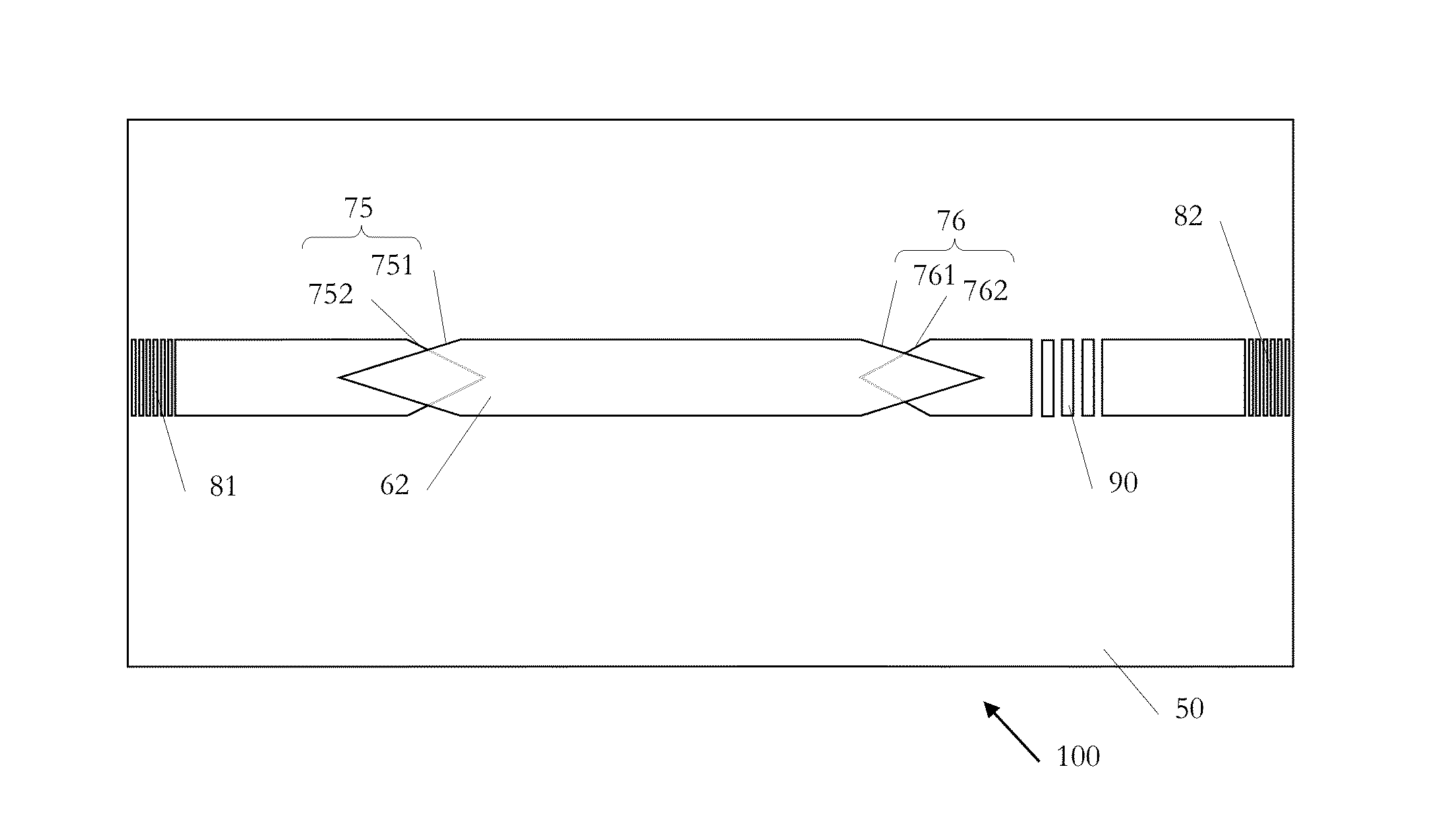
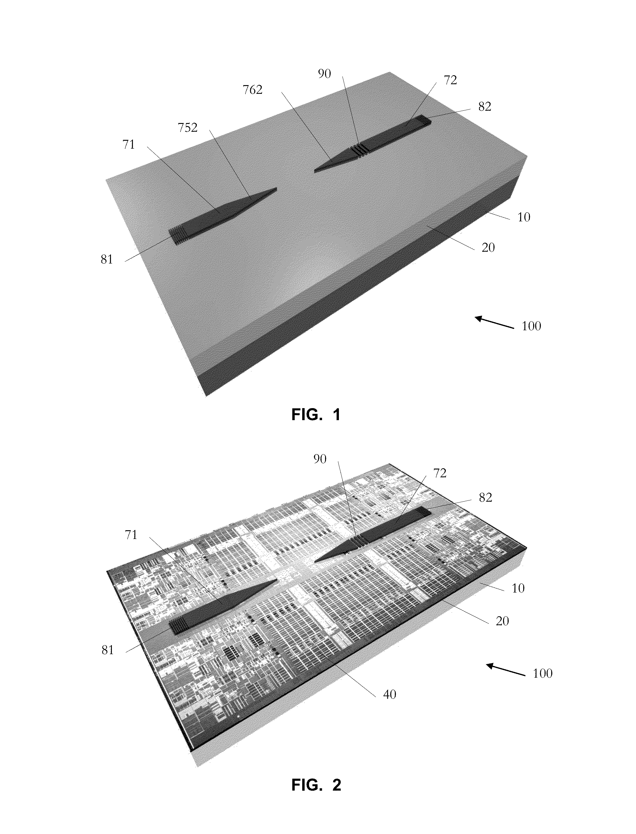
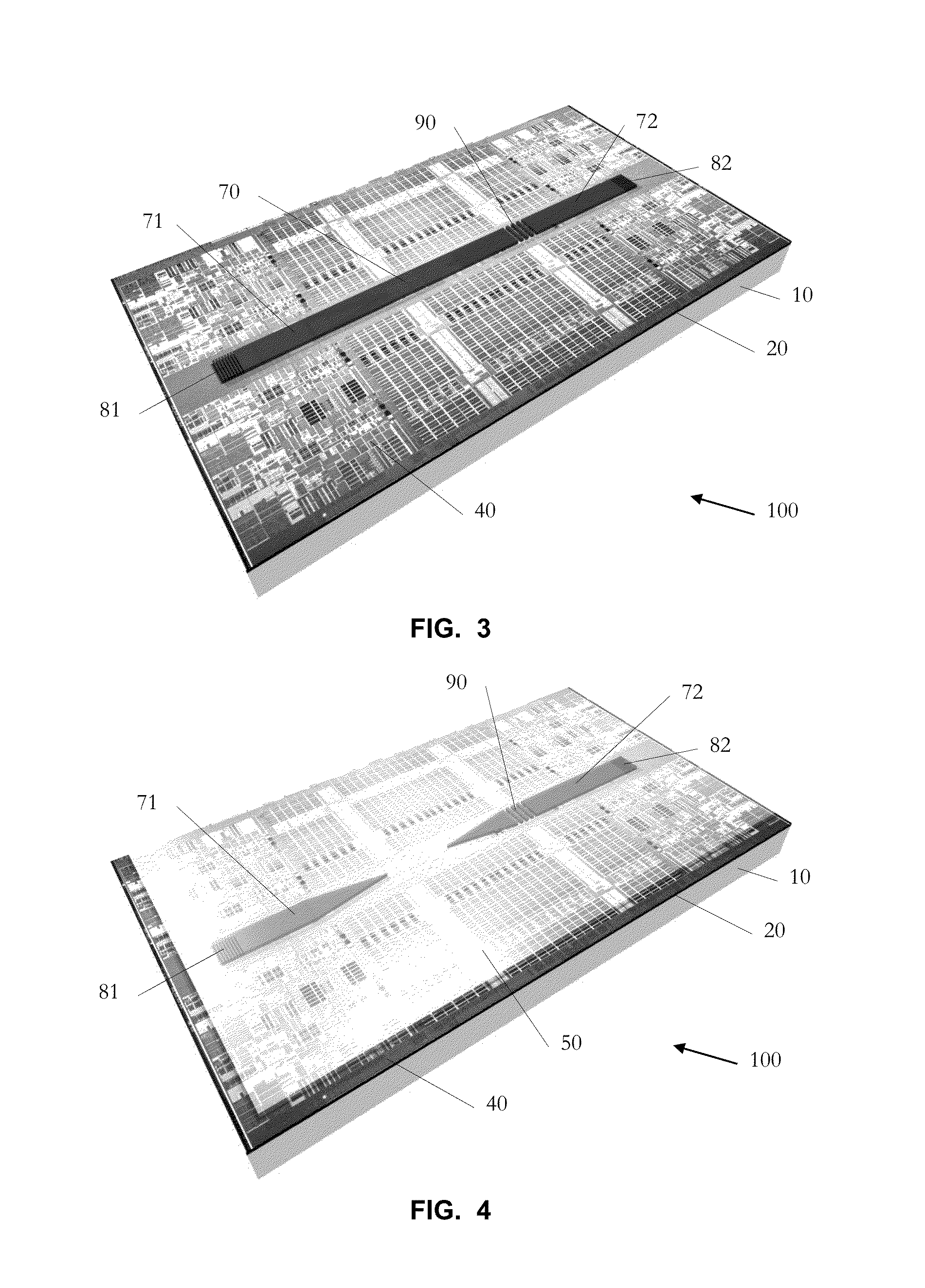
[0071]More specific embodiments and variants thereof are now described. Such embodiments revolve around a device, which resembles a test structure for measuring the on-chip optical gain on a chip, and whose key advantages are that the gain can be measured: By using electrical pumping; By establishing two contacts only and at once; By using vertical fiber probing (thus enabling wafer-scale testing); Without facet polishing; Without fabricating and measuring numerous test structures (one device suffices); Without having to apply numerous (>2) contacts; and Without requiring high spectral resolution.

[0072]An integration scheme is disclosed, where an optically active based gain section made of Germanium, GaAs, InP, InGaAs, InAlAs, InGaAsP, NAsP, GaSb, any of their alloy, or any other suitable compound semiconductor, is evanescently coupled to a waveguide, or forms a hybrid mode with a waveguide, preferably made from silicon. This i...


PUM


Abstract

The present invention is directed to a photonic circuit device for optical gain measurement, including: a substrate with a photonic circuit; an active gain section; at least two light couplers arranged such that at least a part of the active gain section is between the light couplers; and a partial reflector arranged to reflect light propagating along the same direction back to a center of the gain section, and wherein the device does not include any other reflector opposite to the partial reflector with respect to the active gain section and configured to reflect light back to the center of the gain section. The present invention is further directed to related gain measurement methods.

Description

CROSS-REFERENCE TO RELATED APPLICATION[0001]This application claims priority under 35 U.S.C. §371 from PCT Application PCT / IB2014 / 065105, filed on Oct. 7, 2014, which claims priority from United Kingdom Patent Application No. 1319207.5 filed Oct. 31, 2013. The entire contents of both applications are incorporated herein by reference.FIELD OF THE INVENTION[0002]The invention relates in general to the field of photonic circuit devices and, in particular, to optical gain measurement.BACKGROUND[0003]Silicon photonics relate to photonic systems, where silicon is used as medium for light propagation because of the material's low loss. Silicon photonics makes use of well-established silicon manufacturing principles exploited in complementary metal-oxide semiconductor (CMOS) electronics. The features are usually patterned into micro-photonic components with sub-micron precision (to operate in the infrared). Silicon on insulator (SOI) is typically used as a material of choice. The fabricatio...

Claims


Application Information

Patent Timeline
Patent Type & Authority Applications(United States)
IPC IPC(8): G02B6/42G02B6/122G02B6/34H01S5/30H01S5/343H01S5/026H01S5/04H01S5/042H01S3/091H01S3/10H01S5/0683G02B6/12G01J1/44
CPCG02B6/4286G01J2001/4247G02B6/12004G02B6/1228G02B6/34G02B6/428H01S5/3013H01S5/343G01J1/44H01S5/041H01S5/042H01S3/091H01S3/10015H01S5/0683H01S5/026G02B6/4214H01S5/0014H01S5/005H01S5/1032H01S5/50
Inventor HOFRICHTER, JENS
Owner IBM CORP
Why Eureka
Try Eureka