Apparatus and method for light-irradiation heat treatment

Active Publication Date: 2017-01-12
SCREEN HLDG CO LTD
View PDF2 Cites 81 Cited by
  • Summary
  • Abstract
  • Description
  • Claims
  • Application Information

AI Technical Summary

Benefits of technology

[0019]Accordingly, an object of the present invent

Problems solved by technology

At this time, if the annealing time becomes about several seconds or longer, the doped impurities are deeply diffused by heat, and as a result, the junction depth may become too deeper than required and hinder the formation of a good device.
When flash light is applied for heat treatment to this type of semiconductor wafer containing films, an inner wall of a chamber accommodating the semiconductor wafer, an

Method used


Image

  • Apparatus and method for light-irradiation heat treatment
  • Apparatus and method for light-irradiation heat treatment
  • Apparatus and method for light-irradiation heat treatment

Examples


Example

[0028]Hereinafter, a preferred embodiment of the present invention will be described in detail with reference to the drawings.

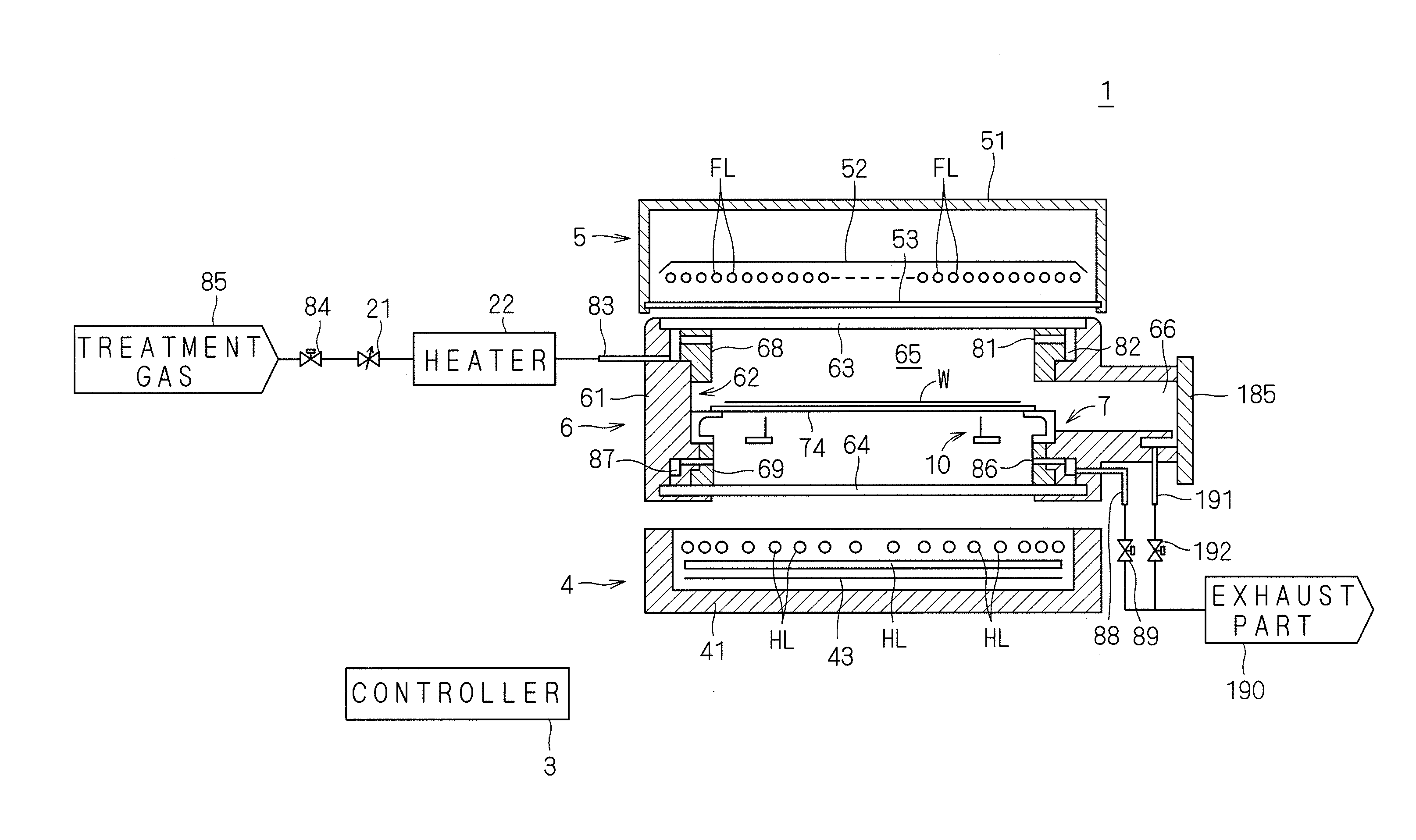
[0029]FIG. 1 is a longitudinal cross-sectional view illustrating a configuration of a heat treatment apparatus 1 according to the present invention. The heat treatment apparatus 1 of this preferred embodiment is a flash-lamp annealing apparatus for heating a disk-shaped semiconductor wafer W as a substrate by irradiating the semiconductor wafer W with flash light. The size of the semiconductor wafer W to be treated is not particularly limited. For example, the semiconductor wafer W has a diameter of 300 mm or 450 mm. The semiconductor wafer W is doped with impurities before being transported into the heat treatment apparatus 1, and the doped impurities are activated through heat treatment by the heat treatment apparatus 1. To facilitate understanding, the dimensions and number of each part are exaggerated or simplified as necessary in FIG. 1 and subsequent dr...


PUM


Abstract

Light is applied for preheating from a halogen lamp to a lower surface of a semiconductor wafer supported on a susceptor within a chamber. Thereafter, flash light is applied for flash heating from a flash lamp to an upper surface of the semiconductor wafer. Treatment gas supplied from a gas supply source is heated by a heater, and supplied into the chamber. A flow amount control valve is provided to increase a flow amount of the treatment gas supplied into the chamber. Contaminants discharged from a film of the semiconductor wafer during heat treatment are discharged to the outside of the chamber with a gas flow formed by a large amount of high-temperature treatment gas supplied into the chamber to reduce contamination inside the chamber.

Description

BACKGROUND OF THE INVENTION[0001]1. Field of the invention[0002]The present invention relates to a heat treatment apparatus and a heat treatment method for heating a sheet precision electronic substrate (hereinafter, simply referred to as a “substrate”), such as a semiconductor wafer, by irradiating the substrate with light.[0003]2. Description of the Background Art[0004]In the process of manufacturing a semiconductor device, the introduction of impurities is an essential step for forming pn junctions in a semiconductor wafer. At present, it is common to introduce impurities by ion implantation and subsequent annealing. Ion implantation is a technique for physically doping impurities by causing impurity elements such as boron (B), arsenic (As), or phosphorus (P) to be ionized and collide with a semiconductor wafer with a high acceleration voltage. The doped impurities are activated by annealing. At this time, if the annealing time becomes about several seconds or longer, the doped i...

Claims


Application Information

Patent Timeline
IPC IPC(8): H01L21/225H01L21/67H01L21/324H05B3/00
CPCH01L21/2253H01L21/324H01L21/67115H05B3/0047H01L21/48H01L21/67098H01L21/67109
Inventor TANIMURA, HIDEAKIMATSUO, KAORUFUSE, KAZUHIKOKATO, SHINICHI
Owner SCREEN HLDG CO LTD
Why Eureka
Try Eureka