Printable component structure with electrical contact

a technology of printed components and electrical contacts, which is applied in the direction of sustainable manufacturing/processing, instruments, and final product manufacturing, etc., can solve the problems of waste of materials, low performance of above-the-line techniques, and low performance of other integrated circuits, so as to achieve simple and inexpensive electrical interconnection process and reduce process steps

Active Publication Date: 2017-02-16
X DISPLAY CO TECH LTD
View PDF27 Cites 39 Cited by
  • Summary
  • Abstract
  • Description
  • Claims
  • Application Information

AI Technical Summary

Benefits of technology

[0089]The present invention provides structures and methods that enable the construction of electrical interconnections between small integrated circuits that are transfer printed on a destination substrate. The electrical interconnection process is simple and inexpensive requiring fewer process steps than known alternative methods.

Problems solved by technology

The above techniques have some limitations.
Despite processing methods used to improve the performance of thin-film transistors, such transistors may provide performance that is lower than the performance of other integrated circuits formed in mono-crystalline semiconductor material.
Semiconductor material and active components can be provided only on portions of the substrate, leading to wasted material and increased material and processing costs.
The choice of substrate materials can also be limited by the processing steps necessary to process the semiconductor material and the photo-lithographic steps used to pattern the active components.
For example, plastic substrates have a limited chemical and heat tolerance and do not readily survive photo-lithographic processing.
Furthermore, the manufacturing equipment used to process large substrates with thin-film circuitry is relatively expensive.
However, such substrate materials can be more expensive or difficult to process.
However, these techniques may be limited in the size of the integrated circuits that can be placed.
While this approach can provide substrates with the same performance as integrated circuits, the size of such substrates may be limited, for example, to a 12-inch diameter circle, and the wafers are relatively expensive compared to other substrate materials such as glass, polymer, or quartz.
However, the bonding technique and the processing equipment for the substrates to form the thin-film active components on large substrates can be relatively expensive.
This method may require etching a significant quantity of material, and may risk damaging the exposed TFT array.
These methods, however, may require the patterned deposition of adhesive on the object(s) or on the second substrate.
Moreover, the laser beam that irradiates the object may need to be shaped to match the shape of the object, and the laser abrasion can damage the object to be transferred.
Furthermore, the adhesive cure takes time, which may reduce the throughput of the manufacturing system.
These processes are expensive and require a number of manufacturing steps.
Moreover, the topographical structure of the small integrated circuits over the destination substrate renders the electrical connections problematic, for example it can be difficult to form a continuous conductor from the destination substrate to the small integrated circuit because of the differences in height over the surface between the small integrated circuits and the destination substrate.

Method used


Image

  • Printable component structure with electrical contact
  • Printable component structure with electrical contact
  • Printable component structure with electrical contact

Examples


Embodiment Construction

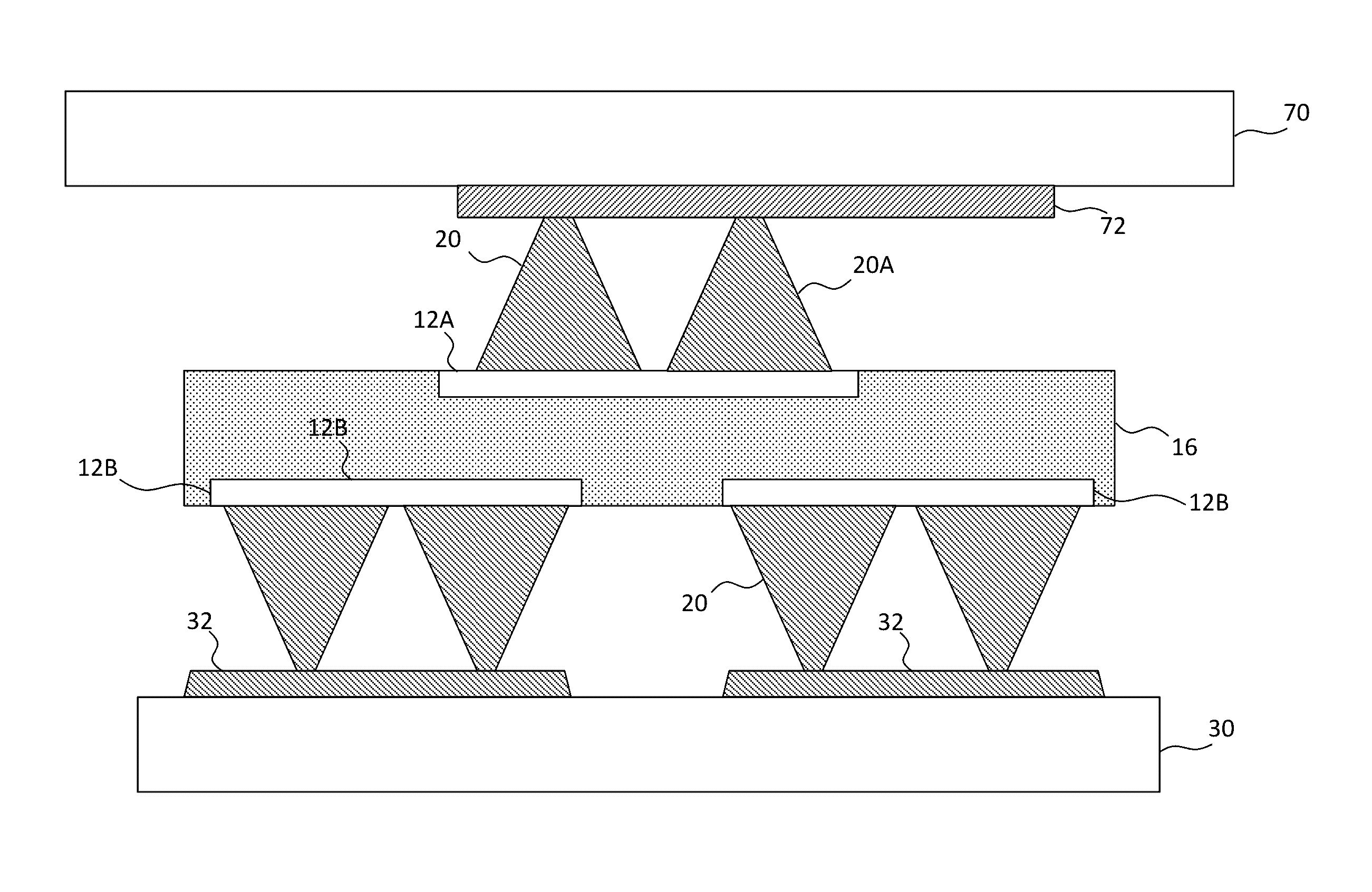
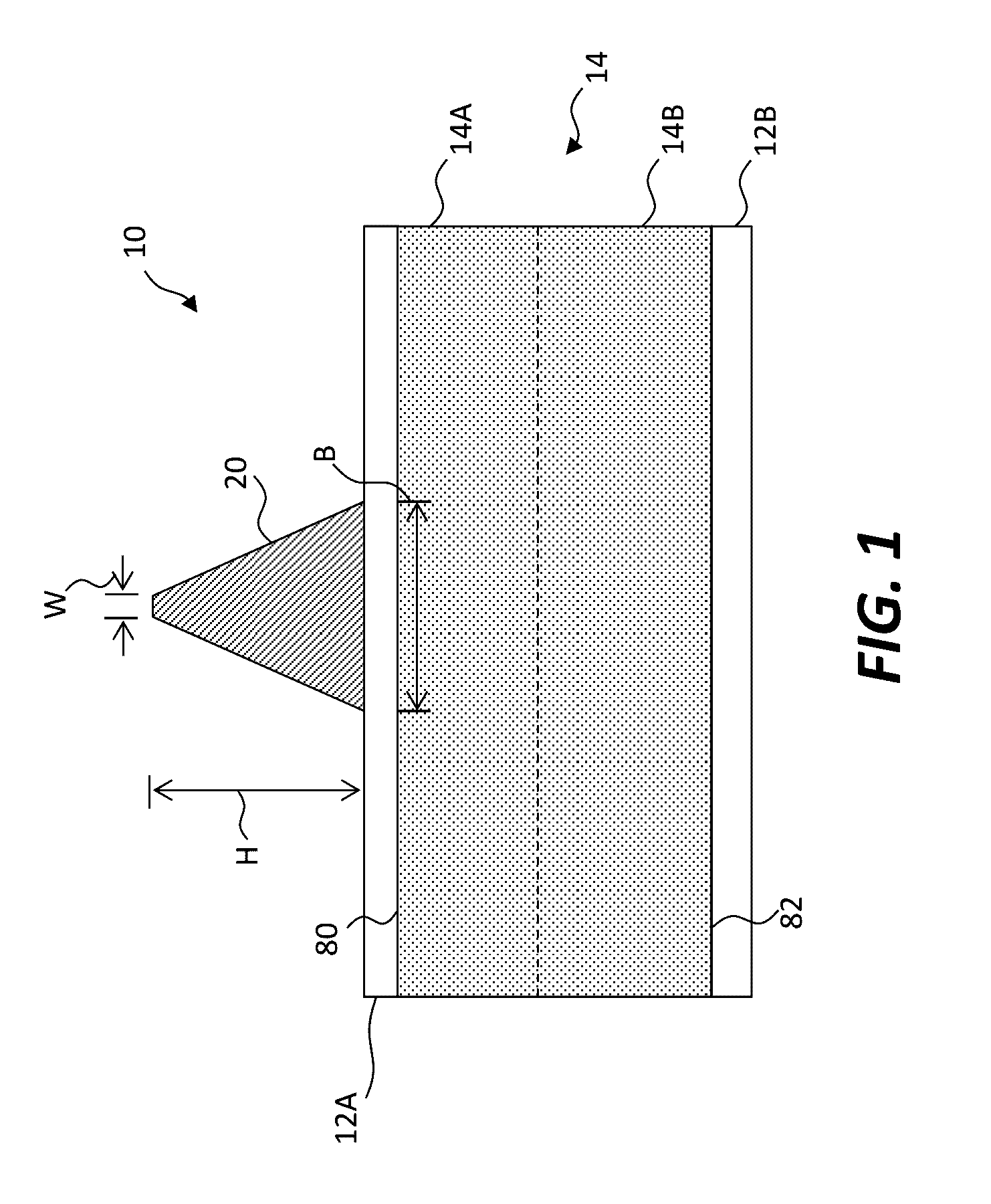
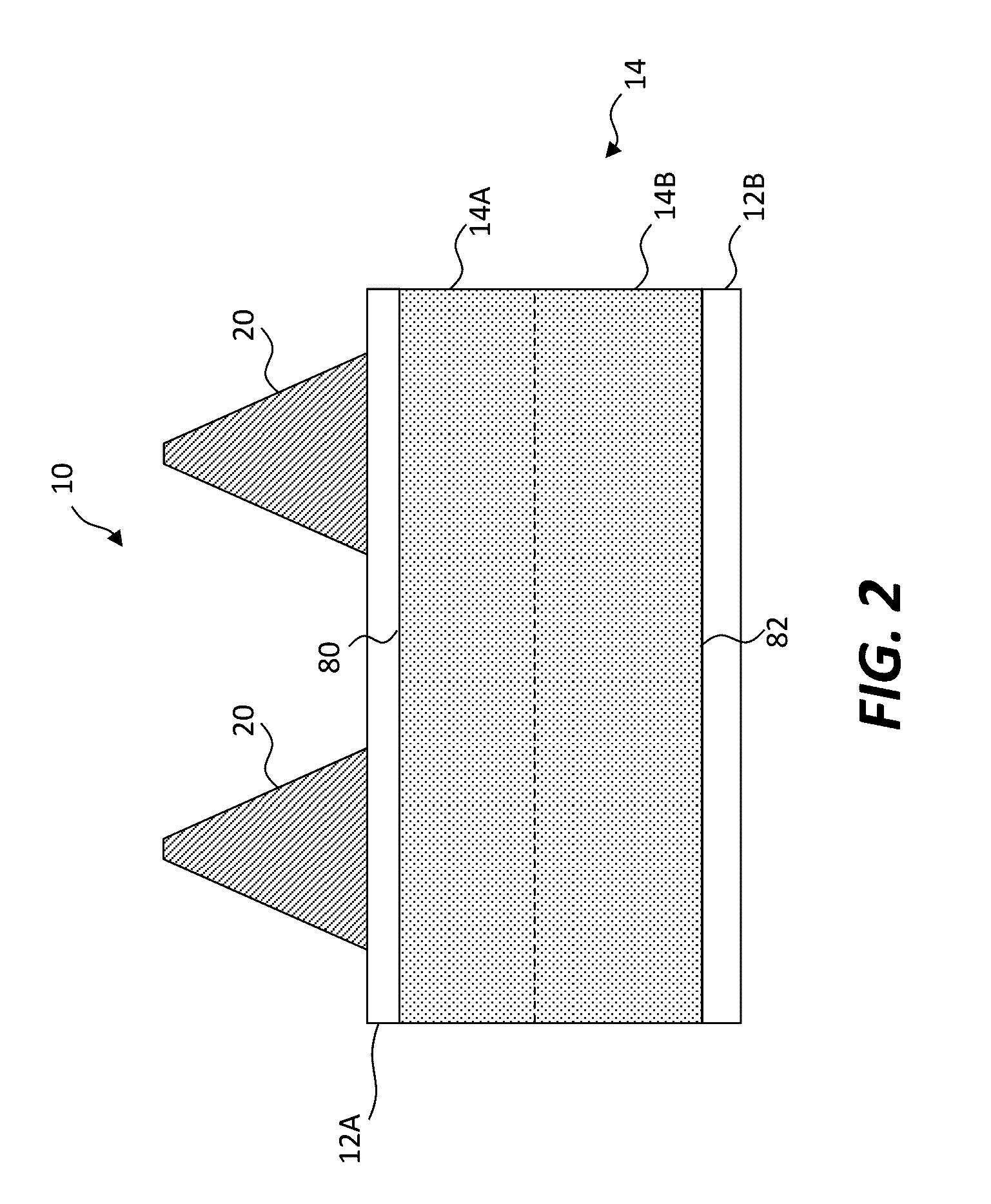
[0106]The present invention provides a structure and method for electrically connecting relatively small electrical components such as integrated circuit chiplets to a common electrical conductor in an efficient and cost-effective way. The common electrical conductor can be a ground plane or power plane. Referring to the cross section of FIG. 1, in an embodiment of the present invention, a printable component structure 10 can be a chiplet that includes a semiconductor structure 14 with a top side 80 and a bottom side 82. One or more top electrical contacts 12A are disposed on the top side 80 of the semiconductor structure 14 and one or more bottom electrical contacts 12B are disposed on the bottom side 82 of the semiconductor structure 14. The semiconductor structure 14 can include a semiconductor substrate. One or more electrically conductive spikes 20 are electrically connected to the one or more top electrical contacts 12A. Each spike 20 protrudes from the top side 80 of the semi...


PUM

PropertyMeasurementUnit
heightaaaaaaaaaa
heightaaaaaaaaaa
heightaaaaaaaaaa

Abstract

A printable component structure includes a chiplet having a semiconductor structure with a top side and a bottom side, one or more top electrical contacts on the top side of the semiconductor structure, and one or more bottom electrical contacts on the bottom side of the semiconductor structure. One or more electrically conductive spikes are in electrical contact with the one or more top electrical contacts. Each spike protrudes from the top side of the semiconductor structure or a layer in contact with the top side of the semiconductor structure.

Description

CROSS REFERENCE TO RELATED APPLICATION[0001]Reference is made to U.S. Pat. No. 8,889,485, entitled Methods for Surface Attachment of Flipped Active Components by Christopher Bower, and to U.S. patent application Ser. No. 14 / 822,864, filed Aug. 10, 2015 and entitled Chiplets with Connection Posts by Prevatte et al, the disclosures of which are incorporated herein by reference in their entirety.FIELD OF THE INVENTION[0002]The present invention relates to structures and methods for electrically interconnecting chiplets using micro transfer printing.BACKGROUND OF THE INVENTION[0003]Substrates with electronically active components distributed over the extent of the substrate may be used in a variety of electronic systems, including flat-panel imaging devices, such as flat-panel liquid crystal or organic light emitting diode (OLED) display devices, and flat-panel solar cells. A variety of methods may be used to distribute electronically active circuits over substrates, including forming t...

Claims


Application Information

Patent Timeline
Patent Type & Authority Applications(United States)
IPC IPC(8): H01L23/00G03F7/20
CPCH01L24/11H01L24/13H01L24/14H01L24/17G03F7/70283H01L2224/1144H01L2224/13023H01L2224/1357H01L2224/1418H01L2224/17107H01L2224/13017H05K3/305H05K3/3436H05K2201/0979H05K2201/10143H05K2201/09472H01L2924/12041H01L2924/12044H01L2924/12043H01L2924/1304H01L2924/14H01L2224/1403H01L2224/1411H01L24/81H01L2224/0401H01L24/05H01L2224/81005H01L24/95H01L2224/95001H01L2224/81191H01L2224/81801H01L2224/81815H01L2224/81193H01L24/06Y02P70/50H01L24/98H01L2224/11612H01L2224/1161H01L2224/1182H01L2224/131H01L2224/136H01L2924/00012H01L2924/01014H01L24/08H01L2224/11466H01L2224/1412H01L2224/16227H01L2224/1624H05K1/112H05K2201/09409
Inventor MEITL, MATTHEWBOWER, CHRISTOPHERCOK, RONALD S.
Owner X DISPLAY CO TECH LTD
Why Eureka
Try Eureka