Method for manufacturing large ceramic co-fired articles

a co-fired ceramic and co-fired technology, which is applied in the manufacture of semiconductor/solid-state devices, basic electric elements, electric apparatus, etc., can solve the problems of warping or unevenness of the clamping surface, eventual cracking of the esc body, damage to the semiconductor wafer, etc., to reduce the number of manufacturing steps in the fabrication process, prevent overheating of the substrate, and high degree of dimensional tolerance

Inactive Publication Date: 2017-03-02
MORGAN ADVANCED CERAMICS
View PDF12 Cites 5 Cited by
  • Summary
  • Abstract
  • Description
  • Claims
  • Application Information

AI Technical Summary

Benefits of technology

[0025]In comparison to roll compaction, dry pressing the ceramic powder formed by powder compaction on uniaxial presses provides more uniform shrinkage, thus making this technique suitable for manufacturing components that not only necessitate a high degree of dimensional tolerance but can be made to relatively large sizes or diameter, e.g. in the manufacture of electrostatic chucks. One example of dry pressing according to one embodiment of the present invention is uniaxial pressing or die pressing or iso-pressing or a combination thereof. Co-firing the laminated assembly provides seamless bonding between the plurality of green compact so creating a monolithic insulating ceramic body with one or more electrical conductors embedded therein.
[0026]Preferably, the step of disposing a conductor or conductor precursor comprises the step of applying a metallization layer to at least one surface of at least one of the plurality of green compacts to form the at least one patterned green compact. Other examples include applying a foil to at least one surface of the green compact or even a conductor precursor such as a printing ink composed of a metal precursor on the layers, e.g. ink jet printing, which subsequently converts to a metallic conductor during firing. Where a fo

Problems solved by technology

Since semiconductor wafers are manufactured to very tight tolerances, any warping or unevenness in the clamping surface of the ESC would be highly undesirable and in an extreme case could even damage the semiconductor wafers.
Other problems encountered in the manufacture of ESCs is the difference in thermal expansion coefficient between the ceramic insulating material and the metal electrodes resulting in stress and eventual cracking within the ESC body when the ESC is operated at high temperatures or thermal cycling.
As wafer size increases, the size of heater and electrostatic chuck to handle wafers also increases, and this larger size is a challenge to the manufacturing of wafer handling devices.
Some of the current wafer heating and chucking apparatus, using glass or low temperature metal bonding, are not able to handle this high temperature requirement.
However, the cost of hot pressing is high in comparison with pressureless sintering methods; in addition, the pressur

Method used


Image

  • Method for manufacturing large ceramic co-fired articles
  • Method for manufacturing large ceramic co-fired articles
  • Method for manufacturing large ceramic co-fired articles

Examples


example 1

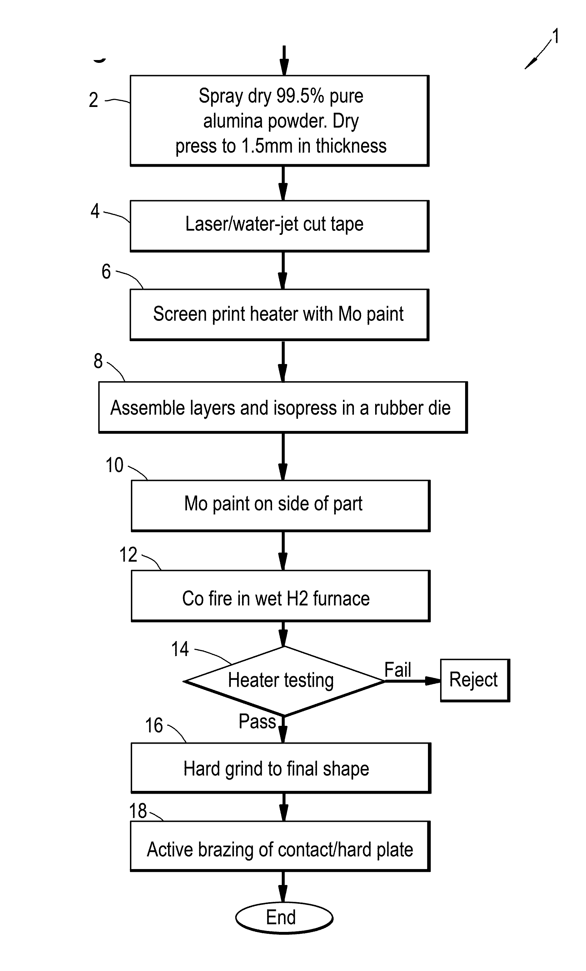
[0066]A multilayer heater is produced using the improved HTCC method as a demonstration of feasibility on a small scale.

[0067]FIG. 1 illustrates the processing flow chart 1 for manufacturing of a four layer heater.

[0068]The process shown uses the spray dried 99.5% pure alumina powder mentioned previously. It should be noted that the present invention is not restricted to 99.5% alumina and can be used for other ceramics, [e.g. alumina of different purity (for example 90-99.9%), ZrO2, Y2O3, AlN, Si3N4, SiC, or indeed any ceramic].

[0069]At step 2, the spray dry powder is pressed (or uniaxially pressed) in a 2″ die to produce thin sheets of about 1.5 mm thickness from the spray dried powder. The dry pressed green sheets is then cut in the green state to the desired shape (Step 4), e.g. by laser or water jet cutting.

[0070]Following cutting of the green sheets, the shaped dry pressed green sheets are metallized to deposit a metallization layer or metallic precursor on its surface (Step 6)...

example 2

[0075]The objective of the example is to demonstrate the new HTCC processing method can be used to produce large sized wafer processing apparatus such as heater and electrostatic chuck (ESC) combination or electrostatic chuck (ESC). The goal is to ensure the 300 mm heater is capable of thermal cycling between room temperature and 600° C. with good temperature uniformity.

[0076]FIG. 3 illustrates the flowchart of the manufacturing process 30. Similar to example 1, the manufacturing process for a 300 mm wafer heating device starts with spray drying of 99.5% pure alumina powder using the alumina powder (Step 32) as mentioned previously.

[0077]The spray dried powder is dry pressed using a 2500 ton dry press (uniaxial press) with an 81 cm diameter die to generate green sheets of 81 cm diameter with thickness in the range of about 2.5 mm to 6 mm (Step 34). In the particular embodiment where the ESC is used in combination with a heater, the combination may be based on assembling three dry pr...


PUM

PropertyMeasurementUnit
Lengthaaaaaaaaaa
Lengthaaaaaaaaaa
Fractionaaaaaaaaaa

Abstract

A method of forming one or more high temperature co-fired ceramic articles, comprising the steps of: —a) forming (34) a plurality of green compacts, by a process comprising dry pressing a powder comprising ceramic and organic binder to form a green compact; b) disposing (38) a conductor or conductor precursor to at least one surface of at least one of the plurality of green compacts to form at least one patterned green compact; c) assembling the at least one patterned green compact with one or more of the plurality of green compacts or patterned green compacts or both to form a laminated assembly; d) isostatically (40) pressing the laminated assembly to form a pressed laminated assembly; e) firing (42) the pressed laminated assembly at a temperature sufficient to sinter the ceramic layers together.

Description

FIELD OF THE INVENTION[0001]The present invention relates to an improved high temperature co-fired ceramic (HTCC) processing method capable of producing large size multilayer ceramic devices. A typical application would be in the manufacture of wafer heating and electrostatic static chuck apparatus used in the manufacture of semiconductors.BACKGROUND ART[0002]Many fields of technology require large ceramic bodies having embedded electrical conductors. As a non-limitative example, in semiconductor manufacturing processes, a wafer heating or chucking apparatus may be used. In the processing of semiconductor wafers or displays, a substrate support is used to retain the substrate during a particular manufacturing process such as during chip manufacturing process. The substrate support is commonly known in the art as an electrostatic chuck (ESC) because it electrostatically clamps onto the substrate, e.g. semiconductor wafer during a manufacturing process such as in a physical vapour dep...

Claims


Application Information

Patent Timeline
IPC IPC(8): C04B37/02H05B3/28H01L21/67C04B35/632H01L21/683
CPCC04B37/021C04B35/632H01L21/6833H01L21/67103H05B3/283C04B2235/3217H05B2203/017C04B2237/343C04B2237/403C04B2237/62C04B2237/706C04B2237/704C04B2235/602B32B18/00C04B35/638H01L21/6831C04B2235/9638C04B2235/9615C04B2235/95C04B2235/77C04B2237/562C04B2237/368C04B2237/365C04B2237/366C04B2237/346C04B2237/348C04B2237/34C04B2235/5436C04B2235/5409C04B2235/668C04B2235/6582C04B2235/6562C04B2235/604C04B2235/6028C04B2235/6025C04B2237/68H05B3/143C04B35/64
Inventor AHRENDES, SAMUEL H.HARLAND, GARY D.LEE, CHENGTSINTOMASEK, EDWARDYORK, III, GEORGE ALBERT
Owner MORGAN ADVANCED CERAMICS
Why Eureka
Try Eureka