
Method for forming aluminum nitride-based film by peald

a technology of aluminum nitride and film, applied in the direction of coating, basic electric elements, chemical vapor deposition coating, etc., can solve the problems of low effective dielectric constant of the device itself, less effective dielectric constant of the device, and less satisfactory conventional diffusion barrier layer and etch step layer, etc., to achieve the effect of improving the leakage curren

Active Publication Date: 2017-03-02
ASM IP HLDG BV
View PDF0 Cites 316 Cited by
  • Summary
  • Abstract
  • Description
  • Claims
  • Application Information

AI Technical Summary

Benefits of technology

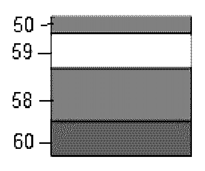
The patent describes a new type of layer made up of two layers - an AlN layer and an AlO layer. This layer is formed using a technique called PEALD and can replace a thinner AlN film. Surprisingly, this new layer has improved leakage current even when it is very thin. This layer can effectively act as a barrier and etch stop layer, replacing the use of an AlN film.

Problems solved by technology

In speed enhancement and energy savings of silicon devices, it is necessary to lower the effective dielectric constant of the devices themselves, and conventional diffusion barrier layers and etch step layers are not satisfactory.
However, when the thickness of a film is in an extremely low range of 3 to 5 nm, the tunnel effect of electrons becomes more significant, and accordingly, the leakage current of the layers increases.

Method used


Image

  • Method for forming aluminum nitride-based film by peald
  • Method for forming aluminum nitride-based film by peald
  • Method for forming aluminum nitride-based film by peald

Examples


examples

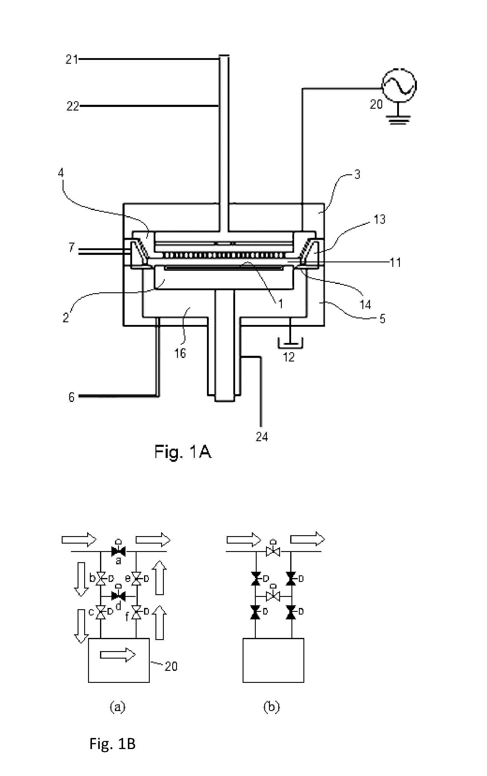
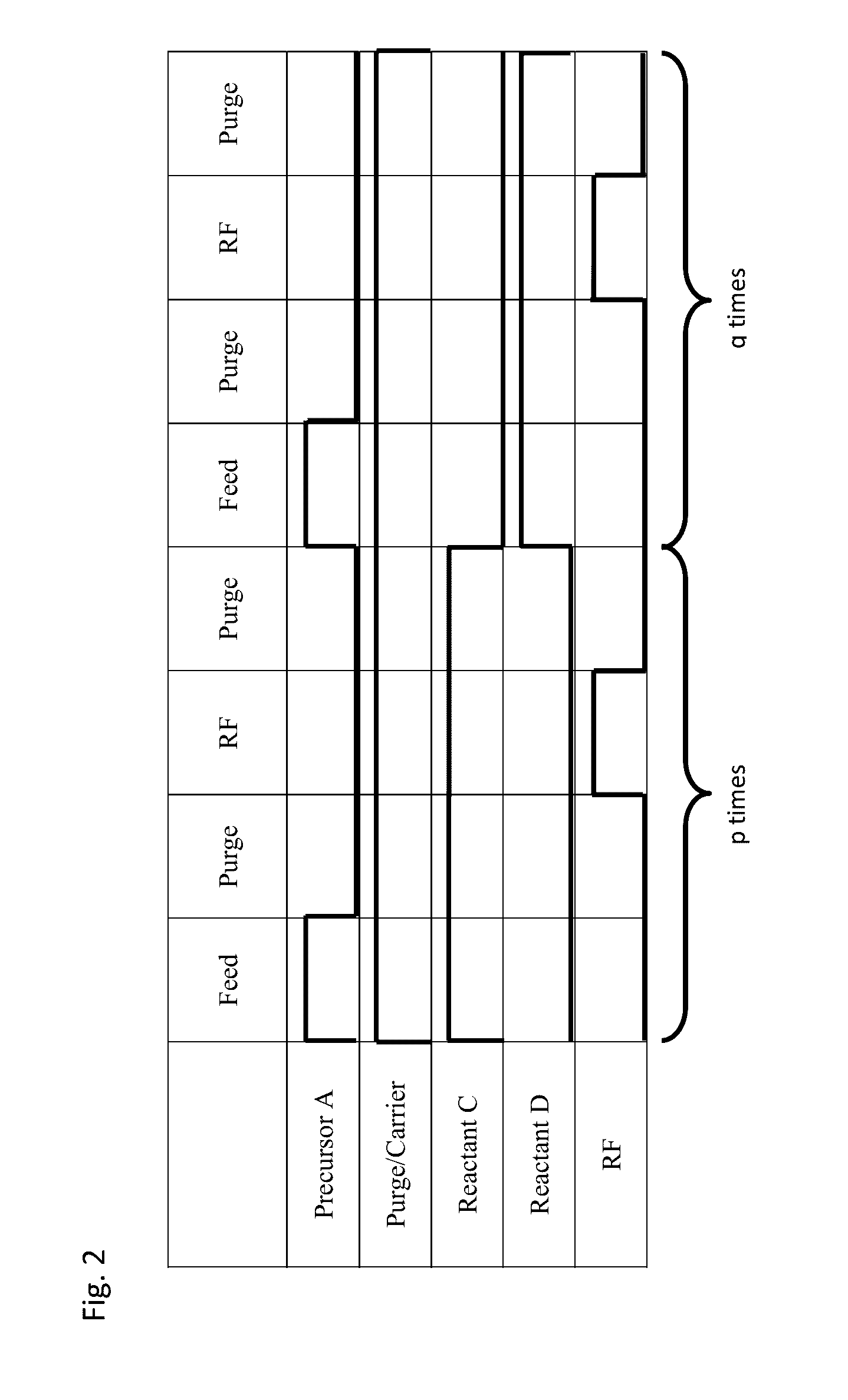
[0046]An aluminum nitride / oxide film was formed on a Si substrate (Φ300 mm) by PEALD, one cycle of which was conducted as illustrated in FIG. 2 under the conditions shown in Table 2 below using the PEALD apparatus illustrated in FIG. 1A (including a modification illustrated in FIG. 1B). The number of each AlN and AlO cycles in each example (Examples a to k) is shown in Table 3. In the examples, TMA (trimethylaluminum) was used as a precursor.

TABLE 2(the numbers are approximate)ProcessAlNAlOPrecurserTMATMAPrecurser Bottle Temp.[deg. C.]3535Carrier Ar ( / RC)[sccm]20002000Dilution Ar( / RC)[sccm]—1000N2 ( / RC)[sccm]3000—H2( / RC)[sccm]100—O2( / RC)[sccm]—2000Seal Ar( / RC)[sccm]200200RC Press[Pa]400300RF(13.56 MHz)[W]300—process temp.[deg. C.]300300TMA feed0.10.1TMA purge0.30.5Deposition Cycle Time [sec]RF On1.01.0Post purge0.10.1Total1.51.7

TABLE 3Exam-1st AlNAlO2nd AlNpleLayer structurecyclecyclecycleaAlN 3 nm5000bAlN 5 nm7000cAlN 10 nm14000dAlN 20 nm28000eAlN 40 nm56000fAlN 3 nm5000gAlO 3 nm02...


PUM

PropertyMeasurementUnit
thicknessaaaaaaaaaa
total thicknessaaaaaaaaaa
thicknessaaaaaaaaaa

Abstract

A method for forming an aluminum nitride-based film on a substrate by plasma-enhanced atomic layer deposition (PEALD) includes: (a) forming at least one aluminum nitride (AlN) monolayer and (b) forming at least one aluminum oxide (AlO) monolayer, wherein steps (a) and (b) are alternately conducted continuously to form a laminate. Steps (a) and (b) are discontinued before a total thickness of the laminate exceeds 10 nm, preferably 5 nm.

Description

BACKGROUND[0001]Field of the Invention[0002]The present invention relates generally to a method for forming an aluminum nitride-based film on a substrate by plasma-enhanced atomic layer deposition (PEALD).[0003]Related Art[0004]Copper (Cu) has been used as a primary wiring material in multilevel interconnection of silicon devices. Since Cu easily diffuses to a transistor layer, an insulating layer, or the like, Ta / TaN or the like is used as a barrier metal layer facing the side and bottom of Cu wiring, and SiN, SiCN, or the like is typically used as a diffusion barrier layer and / or etch stop layer deposited on top of the Cu wiring.[0005]In speed enhancement and energy savings of silicon devices, it is necessary to lower the effective dielectric constant of the devices themselves, and conventional diffusion barrier layers and etch step layers are not satisfactory. There are methods of lowering the effective dielectric constant. For example, by making the diffusion barrier layers and ...

Claims


Application Information

Patent Timeline
Patent Type & Authority Applications(United States)
IPC IPC(8): H01L21/02H01L23/532H01L21/768
CPCH01L21/02178H01L21/02274H01L23/53228H01L21/76834H01L23/53295H01L21/0228C23C16/34C23C16/403C23C16/45529C23C16/45536C23C16/308C23C16/45542H01L21/022H01L21/76832C23C16/52H01L21/28194
Inventor SHIBA, EIICHIRO
Owner ASM IP HLDG BV
Learn More