SEMICONDUCTOR MEMORY DEVICES FOR USE IN ELECTRICALLY ALTERABLE READ ONLY MEMORY (ROM) AND SEMICONDUCTOR THIN FILM DEVICES (SPINTRONS and SPIN-ORBITRONS)

Active Publication Date: 2017-03-09
TROYAN EUGENIY
View PDF1 Cites 10 Cited by
  • Summary
  • Abstract
  • Description
  • Claims
  • Application Information

AI Technical Summary

Benefits of technology

[0071]Ferroelectric phase stability in the nearest zone of the lower memory layer switched to the ON state is characterized by an almost total absence of free carriers the m

Problems solved by technology

However, multiple attempts to create electronic devices on the basis of chalcogenide semiconductors have encountered many difficulties, the most important of which are their instability and unreliability.
Issues related to the physical origin of these metastable states are still under consideration due to their complexity.
The van der Waal's bonds between chains is not very strong.
Te films, produced using vacuum evaporation, have many lattice defects.
And, memory elements were found to be very unstable in the ON state.
Attempting to switch from the OFF to ON state, by supplying a positive potential on the Aluminum electrode, produced thin film structures at U>9-10V inevitably resulted in a break down.
Therefore, creation of adsorbed Oxygen on a Te film's surface leads to a change in the surface's charge.
However, due to the ion's electro-migration, the remaining ions in the complex of positive and negative charges become imbalanced.
Such a valence change is energetically demanding and is a temperature-dependent process.
This leads to the cells instability or metastability, in contrast to the original stable tetrahedral structure where the total number of bondinglike orbitals exceeded the number non-bondinglike ones.
It is known that the change of a charge state of certain impurities in A creates Jan-Tellar local structural instability of AIVBVI complexes due to anharmonicity of cubical potentials.
In contrast with GTS, in STAG compounds it is hard to induce and preserve the necessary polarizing phase without an external electric field.
However, these preconditions are not enough for practical applications because the spontaneous ferroelectric phase created in such chalcogenide compounds a

Method used


Image

  • SEMICONDUCTOR MEMORY DEVICES FOR USE IN ELECTRICALLY ALTERABLE READ ONLY MEMORY (ROM) AND SEMICONDUCTOR THIN FILM DEVICES (SPINTRONS and SPIN-ORBITRONS)
  • SEMICONDUCTOR MEMORY DEVICES FOR USE IN ELECTRICALLY ALTERABLE READ ONLY MEMORY (ROM) AND SEMICONDUCTOR THIN FILM DEVICES (SPINTRONS and SPIN-ORBITRONS)
  • SEMICONDUCTOR MEMORY DEVICES FOR USE IN ELECTRICALLY ALTERABLE READ ONLY MEMORY (ROM) AND SEMICONDUCTOR THIN FILM DEVICES (SPINTRONS and SPIN-ORBITRONS)

Examples


example 1

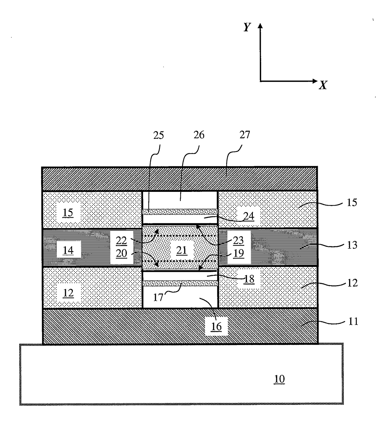
[0098]As shown in FIG. 11, the memory device is formed on an insulator layer 10 which may or may not be a semiconductor substrate. The structure includes an insulator substrate 10, a lower electrode 11 that includes a conductive layer formed from Molybdenum (Mo), a lower Si3N4 insulating layer 12, an offset electrode 13 (or electrodes 13, 14) that includes a conductive layer (or layers) formed from Aluminum (Al), an upper Si3N4 insulating layer 15, a chalcogenide memory material contained in the pore region of the device, and an upper electrode 27 that includes a conductive layer formed from Molybdenum (Mo). The chalcogenide memory material has a stacked structure in which a Tellurium layer (central area) having an appropriate concentration of electrically active donor impurities is placed between two memory layers (lower 19 and upper 23). In the embodiment of FIG. 11, the two interfaces of chalcogenide films, Te—SnTe or Te—GeTe, are used as memory layers 19 and 23 respectively.

[009...

examples 2 and 3

[0114]In these examples, devices having an asymmetric design were fabricated according to the technological process described with respect to Example 1 hereinabove. In the asymmetric design, upper insulating layer 15 and lower insulating layer 12 were of different thicknesses. More specifically, thicknesses of the insulating layers 12 and 15 are such that the offset electrodes 13 and 14 are located in closer spatial proximity to lower memory layer 19 than to upper memory layer 23. The asymmetric placement of electrodes 13 and 14 facilitates the creation of memory cells with effects such as interfacial superconductivity and interfacial magnetization (a current modulation of nonequilibrium magnetization or spin transistor effect) in semiconducting chalcogenide superlattices occurring at room temperature.

example 2

Spin-Orbitrons

[0115]In this example, a layer 21 of Tellurium with a high concentration of mobile positively charged ions is the source of electrically active donor impurities such as the rare earth element Yttrium (Y) and Copper (Cu), or impurities such as iron (Fe) migrating into layers 20 and 22. The amount of the two donor impurities (e.g., Y and Cu) in ion source layer 21 is preferably on the order of approximately 25±10 percent by atomic weight. The content of Copper in the layer 21 is preferably on the order of 4±5 percent by atomic weight. The dielectric layers 17, 25 are used as additives or as the sources of negatively charged impurities in both chalcogenide alloys 18, 24. The thickness of dielectric layers 17, 25 are in the range of 20.0-40.0 nm. The layers 17, 25 of dielectric containing Oxygen and Cuprum (CuO) or Oxygen, Cuprum and Barium (BaCuO2) or even more complex dielectrics, e.g., Lead, Magnesium, Oxygen, Cuprum and Barium {(Pb2Mg2)Ba2Cu9O15} are necessary for the ...


PUM


Abstract

An electrically alterable thin film memory device or non-volatile trigger which can be switched from a high resistance state to a low resistance state. The device increases the concentration of electrically active impurities at correspondent electrodes to which respect impurities would electro migrate during a large number of set-reset cycles. The device comprises a layered structure with memory layers formed on an interface of two regions as the result of the mutual mixing and migration of their constituents. One region contains an electrically active donor impurity. A thin layer of dielectric is placed in the other region. Each of the memory layers includes an interface of chalcogenide films.

Description

CROSS REFERENCE TO RELATED APPLICATIONS[0001]This application is a continuation-in-part (CIP) application claiming priority from U.S. patent application Ser. No. 14 / 618,277 filed Feb. 10, 2015, the disclosure of which is hereby incorporated by reference.STATEMENT REGARDING FEDERALLY SPONSORED RESEARCH OR DEVELOPMENT[0002]N / ABACKGROUND OF THE INVENTION[0003]This invention relates to semiconductor devices; and, more particularly, to semiconductor memory devices used in electrically alterable read only devices or ROMs, and semiconductor thin film devices or spintrons, or spin-orbitrons.[0004]Approximately 60 years ago, the Russian scientist B. T. Kolomiyetz discovered semiconducting features in amorphous chalcogenide compounds. Kolomiyetz, using an external voltage in complex chalcogenide compounds such as AsTeJ, observed the effect of transmission from a high resistance state (OFF) to a low resistance state (ON). This effect was referred to as the effect of threshold switching.[0005]S...

Claims


Application Information

Patent Timeline
IPC IPC(8): H01L45/00
CPCH01L45/1253H01L45/06H01L45/1233H01L45/144H10N70/245H10N70/801H10N70/253H10N70/8828H10N70/826H10N70/841H10N70/231
Inventor TROYAN, EUGENIY
Owner TROYAN EUGENIY
Why Eureka
Try Eureka