Use of etch resist masked anode frame for facilitation of laser cutting, particle and leakage current reduction
- Summary
- Abstract
- Description
- Claims
- Application Information
AI Technical Summary
Benefits of technology
Problems solved by technology
Method used
Image
Examples
example 1
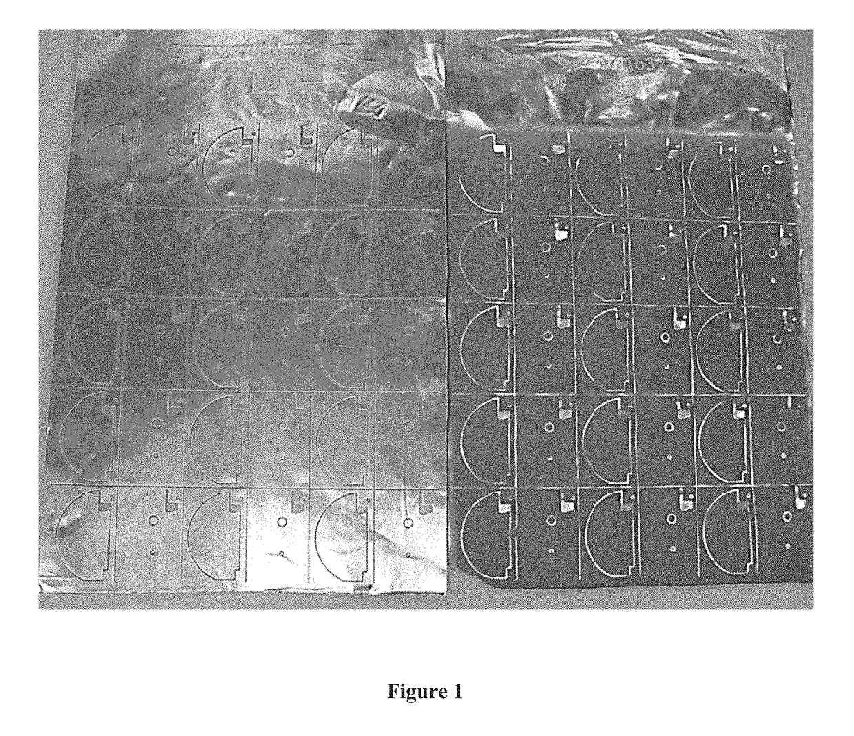
[0040]FIG. 1 demonstrates one example of minimizing the masked surface area. The picture on the left depicts a foil printed with Circuit Jet 200 with a solid frame mask (completely masked) on one side only alternating front to back. The foils without a frame mask in the picture have a frame mask on the back. Alternately, a masked frame may be applied to both sides. The picture on the right shows the foil after it has been etched, the etch resist has been removed, and the foil has been widened and formed as described above. The edges are fully masked on one side and alternate front to back from position to position.
example 2
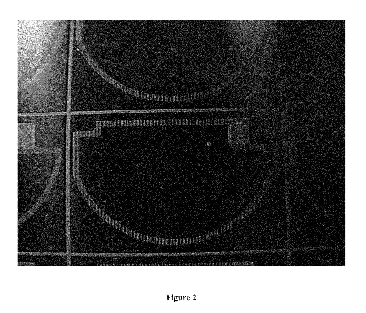
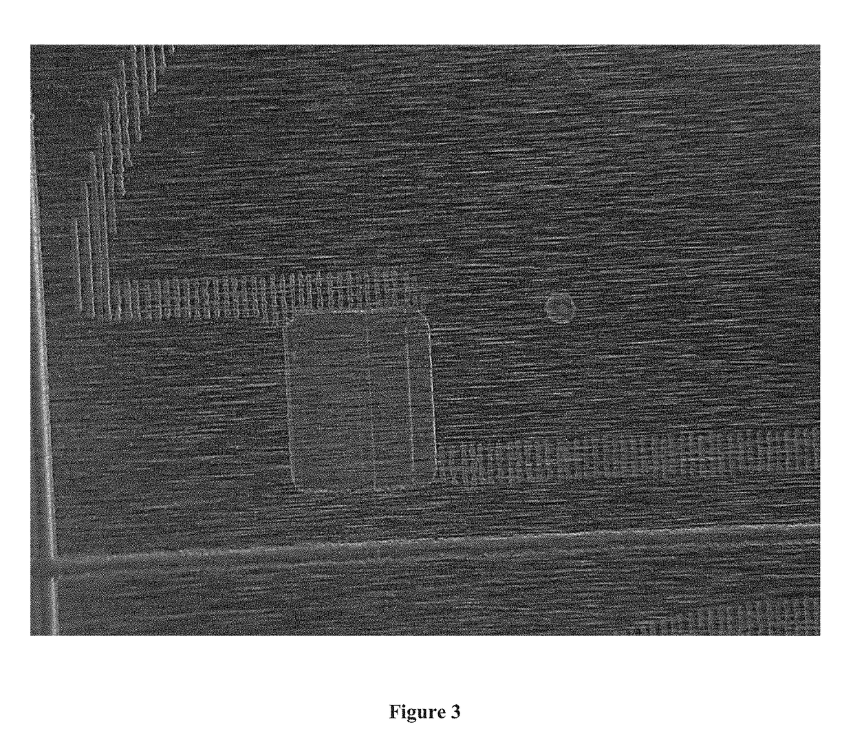
[0041]FIG. 2 shows a close-up of a frame printed mask that is not a solid line. The print line is alternated leaving a 0.01-inch gap between each 0.01-inch line print. FIG. 3 shows a more close up view of the alternating line gaps.
PUM
| Property | Measurement | Unit |
|---|---|---|
| Fraction | aaaaa | aaaaa |
| Electrical resistance | aaaaa | aaaaa |
| Area | aaaaa | aaaaa |
Abstract
Description
Claims
Application Information


