Eureka AIR delivers breakthrough ideas for toughest innovation challenges, trusted by R&D personnel around the world.

Tungsten layer passivation process and direct bonding process

a passivation process and passivation technology, applied in the direction of vacuum evaporation coating, basic electric elements, coatings, etc., can solve the problems of low bonding energy at ambient temperature, difficulty in using the method for bonding substrates comprising components before bonding, and inability to obtain sufficient bonding energies, etc., to increase the conductivity of the bonding layer, increase the bonding energy, and improve the effect of bonding energy

Inactive Publication Date: 2017-07-27
COMMISSARIAT A LENERGIE ATOMIQUE ET AUX ENERGIES ALTERNATIVES
View PDF0 Cites 3 Cited by
  • Summary
  • Abstract
  • Description
  • Claims
  • Application Information

AI Technical Summary

Benefits of technology

The patent describes a method of directly bonding tungsten layers onto substrates using a RF mode of reactive sputtering to avoid poisoning of the tungsten target. This method provides increased bonding energy, reduced defectiveness, and increased conductivity of the bonding layers. The method is quick and inexpensive to implement and includes a heat treatment after the bonding step to further increase the bonding energy and vertical conductivity of the assembly.

Problems solved by technology

One drawback of such a method lies in the fact that it requires the formation of an attachment sublayer (seed layer) for germination in order to form the tungsten layer by CVD.
Another drawback of such a method lies in the fact that the bonding energy is low at ambient temperature.
Another drawback of such a method lies in the fact that the formation of a tungsten layer by CVD is carried out at a temperature above 400° C. and requires densification at a temperature of around 600° C. of the tungsten layer formed.
Such a method may therefore be difficult to use for bonding substrates comprising components before bonding.
However, the known direct bonding methods at ambient temperature and atmospheric pressure of tungsten layers formed by PVD deposition do not make it possible to obtain sufficiently high bonding energies.
Furthermore, defects appear during subsequent heat treatments of the assembly, in particular for temperatures of around 300° C. to 500° C., which corresponds to the temperature ranges normally used during the fracture of a method of the Smart Cut™ type.
These problems of defectiveness and bonding energy are attributed to the presence of an unstable tungsten oxide at the bonding interface.
In all cases, an unstable native tungsten oxide layer is formed on each tungsten layer when the wafers are exposed to ambient air before and during bonding.
The ion bombardment causes an erosion of the surfaces and may, with thin layers (around 10 nm), degrade the conduction properties of the tungsten because of the amorphisation caused.
One drawback of such a process lies in the fact that it is expensive and lengthy to implement.
Furthermore, it requires control of particulate contamination.
In addition, it is difficult to subsequently detach the two tungsten layers, which makes it difficult to recycle the assembled structures in the event of defects.
The problem is also posed of providing a method for the direct bonding of tungsten layers, the bonding layers having reduced resistivity.

Method used


Image

  • Tungsten layer passivation process and direct bonding process
  • Tungsten layer passivation process and direct bonding process
  • Tungsten layer passivation process and direct bonding process

Examples


Embodiment Construction

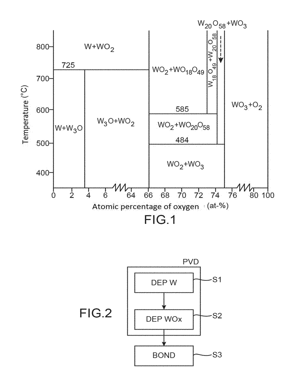
[0064]The inventors propose to carry out an in situ passivation of a tungsten layer formed by physical vapour deposition (PVD). They propose to form a tungsten layer by PVD on a substrate and then, in the same PVD equipment and keeping the substrate under secondary vacuum, to form by reactive sputtering a layer of tungsten oxide WOx with controlled stoichiometry, stable under temperature, on the tungsten layer.

[0065]FIG. 2 is a diagram showing successive steps of a method for the formation and passivation of a tungsten layer by PVD.

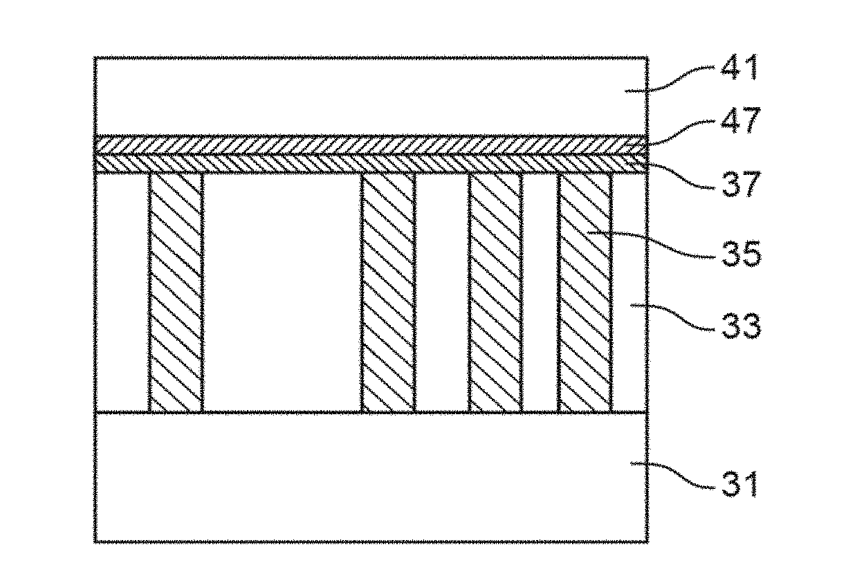
[0066]A tungsten layer is deposited on a substrate, for example made from silicon, by PVD, for example by sputtering (step S1, “DEP W”).

[0067]The deposition of tungsten is carried out in a sputtering chamber of PVD equipment, under vacuum, for example under a high secondary vacuum at 10−7 torr.

[0068]The inert gas used in the working gas plasma is for example argon.

[0069]Optionally, the inert gas may be xenon. The target is a tungsten target.

[0070]The tung...


PUM

PropertyMeasurementUnit
thicknessaaaaaaaaaa
thicknessaaaaaaaaaa
temperatureaaaaaaaaaa

Abstract

A method for forming and passivating a tungsten layer, including: a) depositing, by PVD deposition, a tungsten layer on a substrate; and b) depositing by PVD deposition, a tungsten oxide passivation layer on the tungsten layer, by reactive sputtering in a plasma containing dioxygen, the tungsten oxide layer as deposited being amorphous and having a resistivity of between 5×10⁻² and 5×10⁻³ O·cm, the substrate being kept in an inert atmosphere between a) and b).

Description

TECHNICAL FIELD[0001]The present invention relates to a method for passivating a tungsten layer, and more particularly a method for passivating a tungsten layer formed by physical vapour deposition (PVD). The present invention further relates to a method for the electrically conductive direct bonding of tungsten layers.PRIOR ART[0002]Copper is normally used as a material for forming interconnections. However, the resistivity of copper increases significantly for thin films and fine interconnections. The conductivity of tungsten is then superior to that of copper.[0003]Tungsten also has other advantages compared with copper. One advantage lies in the fact that tungsten is less contaminating than copper. Another advantage is related to the fact that tungsten has a melting point more than twice that of copper (3695 K for tungsten as against 1358 K for copper). As a result tungsten has better resistance to high temperature than copper, which is particularly advantageous for certain appl...

Claims


Application Information

Patent Timeline
Patent Type & Authority Applications(United States)
IPC IPC(8): H01L23/00C23C14/00C23C14/16C23C14/34H01L25/00H01L21/18H01L21/285H01L21/768H01L23/532C22F1/18C23C14/58
CPCH01L24/83C22F1/18C23C14/0036C23C14/165C23C14/3414C23C14/5806H01L21/187H01L21/2855H01L21/76834H01L23/53266H01L25/50H01L21/76898H01L2224/05184C23C14/025C23C14/06C23C14/083H01L24/80H01L2224/05186H01L2224/80896H01L2924/01074H01L2924/00014
Inventor BENAISSA, LAMINEGONDCHARTON, PAULIMBERT, BRUNO
Owner COMMISSARIAT A LENERGIE ATOMIQUE ET AUX ENERGIES ALTERNATIVES
Why Eureka
Eureka Blog
Learn More