

Method of manufacturing hexagonal boron nitride laminates
- Summary
- Abstract
- Description
- Claims
- Application Information
AI Technical Summary
Benefits of technology
Problems solved by technology
Method used
Image


Examples
Embodiment Construction
[0018]A method of manufacturing hexagonal boron nitride laminates according to a preferred embodiment of the present invention contains steps of:
[0019]a) Dissolving 10 to 80 wt % dielectric polymers in solvent.
[0020]Preferably, the dielectric polymer is at-least one of the following polymers, including polyethylene terephthalate (PETP), polyphenylene sulfide (PPS), polyetherimide (PEI), polyetherether ketone (PEEK), polyetherketone (PEK), polyimide (PI), Polyvinylidene fluoride (PVDF), phenol resin or acrylic resins.
[0021]b) Mixing 20 to 90 wt % h-BN powder to form a well-mixed h-BN coating slurry.
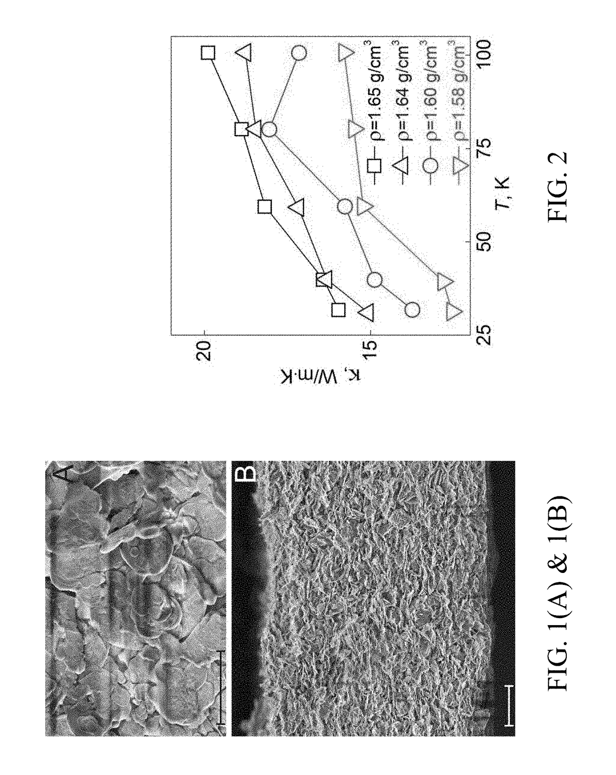
[0022]Preferably, the thickness of h-BN powders ranges from 1 to 500 nm, and the size is from 0.1 to 100 μm.
[0023]c) Coating slurry on substrates and dried at 100 to 150° C. A layer of h-BN laminates was obtained after this process.
[0024]d-1) For free standing h-BN film, peel off h-BN dielectric polymer layer from substrate in water batch by roll to roll process.
[0025]d-2) For h-BN film on...
PUM
| Property | Measurement | Unit |
|---|---|---|
| Temperature | aaaaa | aaaaa |
| Temperature | aaaaa | aaaaa |
| Length | aaaaa | aaaaa |
Abstract
Description
Claims
Application Information